TIDA-010210 11kW bidirectional three-phase GaN-ANPC
1. Design Overview
TIDA-010210 is a reference design for an 11kW bidirectional three-phase three-level ANPC inverter released by Texas Instruments. The core uses GaN power devices to achieve 100kHz high-frequency switching, specifically designed for photovoltaic inverters, DC charging stations, and power conversion systems (PCS), balancing high power density, high efficiency, and bidirectional power transmission capability.
2. Core system parameters
Key Explanation of Parameter Specifications
Output power 11kW, three-phase 400V AC rated output
AC rated voltage three-phase 400V AC 50/60Hz power frequency
Output current 16A AC side rated current
DC bus voltage 600-800V DC nominal 800V
Switching frequency 100kHz GaN high-frequency switching characteristics
Peak efficiency 98.5% 400V AC, 60% load point
Power density 2.57kW/L, overall volume 4.29L
Bidirectional commutation time<1ms, fast switching of power flow direction
3. Topology and Device Selection
Topology structure: Adopting a three-level ANPC topology, the device voltage stress is limited to 1/2600V of the DC bus, and the device can be adapted to 800V bus.
Power devices:
High frequency switch (Q1/Q5/Q4/Q6): GaN device LMG3422R030 (600V/30m Ω), with no reverse recovery loss.
Low frequency switch (Q2/Q3): Si MOSFET (650V/40m Ω), 100/120Hz power frequency switching.
Main control and driver:
Main controller: TMS320F280049C (C2000 series), CLB implements hardware protection.
Driver: UCC21541 isolated driver, built-in driver for GaN devices.
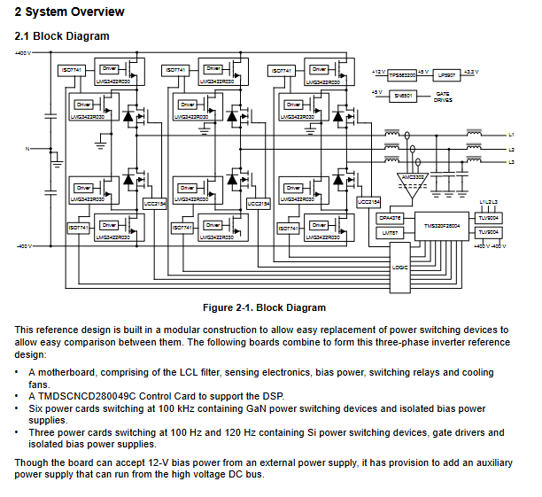
4. Hardware architecture composition
Motherboard: Integrated LCL filter, sampling circuit, auxiliary power supply, relay, and cooling fan.
Power board: 6 GaN high-frequency power boards (100kHz)+3 Si low-frequency power boards (100/120Hz).
Control card: TMDSCNCD280049C, providing DSP control and PWM output.
Auxiliary power supply: External 12V input, converted from TPS563200 to 5V, LP5907 to 3.3V; SN6501 generates isolated driving power supply.
5. Key circuit design
LCL filter:
Inverter side inductance: 360 μ H, grid side inductance: 15 μ H, filter capacitor: 4.7 μ F.
Resonant frequency: 19.35kHz, meets stability requirements, damping resistance 0.58 Ω.
Sampling circuit:
Voltage sampling: TLV9004 operational amplifier, resistor divider+1.65V bias, compatible with MCU ADC.
Current sampling: AMC3302 isolated sampling, 2m Ω shunt resistor, ± 50mV input, low loss and high precision.
Protection design: Based on C2000 CLB, hardware interlock protection is implemented without additional device costs to prevent overvoltage damage.
6. Control and functional advantages
PWM optimization: Only 6 PWM channels are required, while traditional solutions require 9 channels, reducing MCU resource consumption.
Bidirectional operation: The hardware naturally supports bidirectional operation of inverters/PFCs, requiring only software switching.
High reliability: Low device voltage stress, reducing the risk of failure.
Low cost: Each phase bridge arm only has 4 high-frequency switches, while traditional solutions require 6.
7. Test results
Inverter mode: Output pure sine wave under 800V bus, with no significant distortion at zero crossing.
PFC mode: Full load THD<4%, efficiency ≥ 98% under 600V/800V bus, peak value 98.62%.
Dynamic performance: current 1A ↔ 6A transient response is smooth and the loop is stable.
8. Application scenarios
Photovoltaic string inverter
DC wall mounted charging station
Energy Storage Power Conversion System (PCS)