ADLINK NuDAQ 7200 series high-speed digital I/O board
Product Overview
1.1 Core Hardware Specifications
1. * * Channel configuration * *: Unified 32 channels of TTL digital input DI and 32 channels of TTL digital output DO; cPCI version additionally comes with 4 channels of auxiliary input AUXIN and 4 channels of auxiliary output AUXOUT.
2. * * Transmission performance**
-Peak transmission rate of 12MB/s (3MHz clock, external clock/handshake mode); The maximum internal timer mode is 8MB/s (2MHz).
-Using PCI bus for main DMA transmission, there is no need for CPU to frequently transfer data.
3. * * onboard storage FIFO**
-PCI/PCIe-7200: 8 32-bit word FIFOs for input and output respectively;
-CPCI-7200: Input additional 2K dual word large capacity FIFO, high-speed continuous acquisition is more stable.
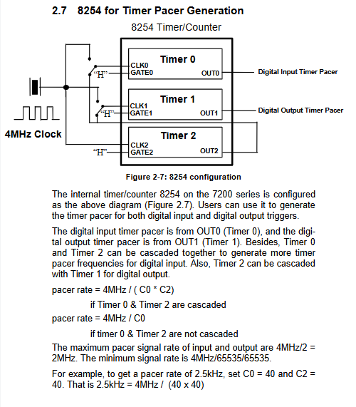
4. * * Timer Unit * *: Equipped with 82C54-10 timer counter, 4MHz reference clock, and 3 independent timers:
-Timer0: Digital input sampling clock; Timer1: Digital output triggers clock; Timer2: Reference frequency division, capable of cascading and expanding frequency range;
-Clock output range: 0.00046Hz~2MHz.
5. * * Electrical level (TTL standard)**
-Input: Low level 0~0.8V, high level ≥ 2.0V;
-Output: Low level maximum current of 24mA, high level pulling current of 3mA, output high level ≥ 2.7V;
6. * * Bus and structure differentiation**
|Model | Bus specifications | Dimensions | Power supply | Interface connectors | Input terminals|
|PCI-7200 | Universal 3.3V/5V PCI | 148 × 102mm |+5V 720mA | 37 pin D-Sub (CN2)+40 pin ribbon socket (CN1) | No pull-up/termination|
|PCIe-7200 | x1 PCIe | 168 × 111mm |+12V 200mA,+3.3V 500mA | 37 pin D-Sub+40 pin cable tray | No pull/terminal|
|CPCI-7200 | 3U CompactPCI PICMG2.0 | Standard 3U Eurocard |+5V 820mA | 100 pin SCSI integrated interface | Schottky diode clamp terminal|
7. * * Environmental indicators * *: Operating at 0-60 ℃, storage at -20~80 ℃, humidity at 5%~95%, no condensation.
1.2 Four major working modes
1. * * Direct Program Control Mode * *: Software directly reads and writes IO registers, suitable for low-speed discrete IO control;
2. * * Internal timer beat mode * *: 8254 timed trigger sampling/output, DMA batch transfer, suitable for fixed frequency continuous acquisition;
3. * * External clock mode * *: External I-REQ signal locks input data, triggered synchronously by external devices;
4. Handshake mode: EQ/ACK response signal, synchronized upstream and downstream devices, the only mode that can ensure data integrity at high speeds.
1.3 Typical application scenarios
High speed peripheral docking, cross device high-speed data exchange, digital IO automation control, external AD/DA high-speed synchronization, digital waveform/pulse signal generator.
1.4 Supporting software ecosystem
All software is integrated on the Linghua All in One CD, supporting the full range of Windows 32/64 bit systems (98/NT/2000/XP/Vista/Server):
1. * * DAQPilot (mainly promoting the new generation of drivers)**
Task oriented collection SDK, graphical interface, supports LabVIEW, MATLAB, C #/C++/VB/Delphi development, simplifies programming, officially recommended for priority use;
2. **DAQMaster**
Equipment management configuration tool, integrating hardware parameter settings, task management, calibration, and driver upgrades;
3. PCIS-DASK (Traditional Legacy Driver)**
Bottom level kernel driver, suitable for deep customized development; Provide digital signatures that are compatible with Vista 64 bit and WOW64 to enable 32-bit programs to run on 64 bit systems; The official suggestion is to avoid using it in new projects.
4. Supporting components: ActiveX controls,. NET assemblies, LabVIEW VI library, MATLAB specialized toolkit.
Hardware Installation Chapter
2.1 Packaging List
Board body, supporting cables (PCI/PCIe with ACL-10437 40 to 37 pin data cable), user manual, software installation CD; Contact the dealer for missing accessories.
2.2 Anti static operation specifications
Grounding anti-static pads on the workbench and wearing anti-static wristbands; After opening the box, avoid touching the chip and do not turn on the power if it is damaged.
2.3 Plug and play resource allocation
No jumper/dip switch; Interrupt numbers and IO base addresses are automatically assigned by the motherboard BIOS, and it is not recommended to manually modify resources.
2.4 Hardware installation steps
1. Power failure of the entire machine and external devices;
2. Open the computer case and touch the metal casing to release static electricity;
3. Insert the corresponding PCI/PCIe/cPCI slot and secure the baffle;
After booting up, Windows automatically recognizes new hardware and installs drivers according to the instructions on the CD.
2.5 Definition of connector pins
1. PCI/PCIe dual interfaces:
-CN2 (rear 37 pin D-Sub): DI0~DI15, DO0~DO15, handshake I-REQ/I-ACK, external trigger I-TRG,+5V, GND;
-CN1 (onboard 40 pin ribbon cable): DI16~DI31, DO16~DO31, output trigger O_TRG, O-REQ/O_CK;
2. cPCI-7200 single 100 pin SCSI interface: integrates all 32DI/32DO, 4-channel auxiliary IO, all handshake/trigger signals, and power ground.
2.6 8254 Timer Cascade Rules
The reference 4MHz clock can be cascaded with Timer0/Timer2 or Timer1/Timer2 to reduce the output frequency; Calculation formula:
-Not cascaded: beat frequency=4MHz/counter initial value;
-Two level cascade: beat frequency=4MHz/(C0 × C2);
Example: 2.5kHz output configuration C0=40, C2=40.
2.7 Differences in Input Terminal Circuits
PCI/PCIe does not have built-in terminal resistors; CPCI is equipped with Schottky diode clamp circuit to suppress high-speed signal reflection overshoot/undershoot.
Register Address and Definition
3.1 IO Address Mapping
-PCI/PCIe: 8 consecutive 32-bit IO addresses (Base+0~Base+1C);
-CPCI: Additional Base+20 auxiliary IO registers, totaling 9 32-bit addresses;
**Restriction: Only supports 32-bit read and write, prohibits 8/16 bit single byte access.
3.2 Core Register Function
1. * * Base+10 digital input register (read-only) * *: reads 32 real-time DI levels;
2. * * Base+14 digital output register (read-write) * *: Set 32 DO channels and support reading back the current output status;
3. * * Base+18 DIO Status Control Register * *: Configure four working modes, FIFO switch, trigger polarity, overflow/underflow status bits (I-OVR input overflow, O-UNUD output underflow, write 1 to reset);
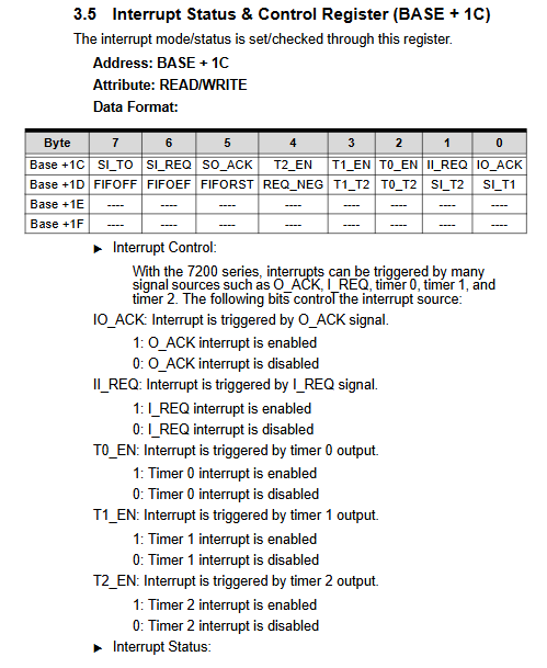
4. * * Base+1C interrupt status control register * *:
-Interrupt source enable: I-REQ, O-ACK, Timer0/1/2;
-Interrupt status flag: corresponding to interrupt triggered after 1, write 1 to clear;
-Timer cascade switch, I-REQ triggering edge selection;
-CPCI exclusive: Large capacity FIFO empty/full flag, FIFO reset bit;
5. * * Base+0~Base+C 8254 Timer Register * *: Three counter read/write and clock control words.
Working principle and timing sequence
1. * * Direct IO mode * *: Program loop reads and writes DI/DO registers, without DMA or FIFO, suitable for low-speed point-to-point control;
2. * * Timer beat DMA mode * *: Timing pulse triggers acquisition, data is stored in FIFO, bus DMA automatically uploads to memory, suitable for fixed cycle continuous acquisition;
3. * * External I-REQ trigger mode * *: External device pulse latch DI, DMA batch transfer, external device synchronous acquisition;
4. Handshake transmission mechanism**
-Input handshake: External sends I-REQ → latches DI → board returns I-ACK to inform that external data has been read;
-Output handshake: DMA sends data from memory to FIFO → ready output sends O_ REQ → refreshes the next set of outputs upon receiving external O_ ACK;
5. * * Detailed electrical timing parameters * *: Specify the high and low level holding time, establishment/holding time, and PCI clock cycle requirements for I \ -REQ/O \ -REQ to ensure high-speed signal stability.
Double buffer DMA acquisition principle
Specially designed for continuous and uninterrupted digital input, the circular memory buffer is split in half:
1. The board first fills the first half of the buffer zone; Automatically write to the second half after filling;
2. The application program synchronously reads and processes the first half of the data without interrupting hardware collection;
3. After the second half is filled, the hardware switches back to the first half to overwrite the old data, and the cycle repeats;
4. Advantages: No data interruption, suitable for long-term high-speed continuous acquisition scenarios.
Hardware performance limitations
1. The peak value of 12MB/s can only be reached when the bus is exclusive, and sharing the PCI bus with multiple devices cannot guarantee it;
2. There is a risk of data loss in the internal timer/external clock mode at high speeds (limited FIFO depth, PCI bus delay fluctuations), and only handshake mode can ensure data integrity;
3. Stable and reliable upper limit: 1MB/s when a single card monopolizes the bus;
4. The maximum single DMA transfer capacity is 64MB;
5. cPCI high-capacity FIFO only alleviates overflow and cannot completely eliminate data loss caused by bus preemption.