ADLINK DAQ-20XX/PXI-20XX series 4-channel synchronous multifunctional data acquisition card
DAQ-20XX (PCI)/PXI-20XX (PXI) 4-channel synchronous multifunctional data acquisition card, part number 50-11020-1030. This series includes four models: 2010 (14 bit, 2MS/s), 2005 (16 bit, 500kS/s), 2006 (16 bit, 250kS/s), 2016 (16 bit, 800kS/s); Equipped with synchronous analog input, analog output, digital IO, and universal counter, supporting SSI multi card synchronization, widely used in automotive testing, transient signal measurement ATE、 Scenarios such as biometric measurement and laboratory automation.
Main hardware features
1. Analog input AI (4-channel differential synchronous sampling)
2010: 14 bits without lost codes, maximum 2MS/s; Onboard A/D FIFO 8K samples
2005: 16 bit no code loss, up to 500kS/s; FIFO 512 samples
2006: 16 bit no code loss, up to 250kS/s; FIFO 512 samples
2016: 16 bit no code loss, up to 800kS/s; FIFO 512 samples
Input range: Bipolar ± 10/± 5/± 2.5/± 1.25V; Monopolar 0-10/0-5/0-2.5/0-1.25V; Programmable gain × 1/× 2/× 4/× 8
Protection: Continuous ± 30V overvoltage protection when powered on; Power off ± 15V; input impedance 1G Ω//100pF
Indicators: Provide 3dB small signal bandwidth, system noise, DC-60Hz common mode rejection ratio CMRR; The maximum deviation before calibration is ± 60mV, and after automatic calibration it is ≤ ± 1mV.
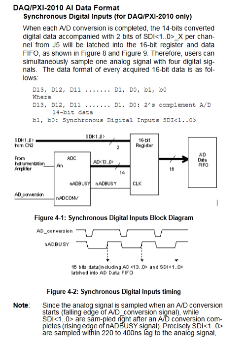
Only the 2010 model has SDI synchronous digital input: each AI channel is accompanied by a 2-bit digital signal, which is synchronously latched into FIFO with analog sampling; No SDI in 2005/2006/2016.
2. Analog output AO (2 channels, 12 bits)
DAC chip LTC7545; Maximum update rate 1MS/s; Output FIFO: Single channel works with 2K samples, dual channel works with 1K samples simultaneously.
Range: Bipolar ± 10V, Unipolar 0-10V; Supports external reference voltage AOEXTREF input.
Electrical: setup time from 3 µ s to 0.5LSB; Voltage swing rate 20V/µ S; output short circuit protection; Maximum driving current ± 5mA; power on output 0V.
3. Digital I/O
Universal DIO (82C55A): 24 channels of TTL/CMOS programmable bidirectional IO, divided into three 8-bit ports: PA, PB, and PC; Each port’s high and low half bytes can be independently configured for input/output; All power on inputs are high impedance.
SDI synchronous digital input (2010 only): 8 channels, captured synchronously with analog sampling, stored in FIFO along with AD samples.
4. Universal Timer/Counter GPTC
2-channel 16 bit up/down counter; The maximum clock is 10MHz; Support internal/external clock sources; Gate, Up/Down can be controlled by software/hardware; Provide 8 working modes: event counting, cycle measurement, pulse width measurement, single pulse, trigger pulse, continuous pulse generation, etc.
5. Trigger and timing
Trigger source: software trigger, external analog trigger, external digital trigger, SSI system synchronization interface trigger.
AI has four collection modes: pre trigger, middle trigger, post trigger, and delay trigger; Support re triggering Re trigger.
Simulate triggering 5 conditions: below low threshold, above high threshold, within interval, high latency, low latency; External EXTATRIG or any AI channel can be selected as the simulation trigger source.
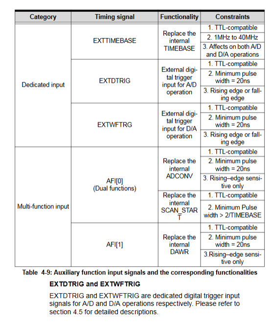
TIMEBASE: onboard 40MHz internal clock; It also supports external EXTTIMEBASE (1-40MHz TTL).
6. SSI system synchronization interface (multi card synchronization)
20 pin SSI interface, supporting one master and multiple slaves (1 master can drive up to 3 slave cards); It can synchronously distribute timebase TIMEBASE, ADCONV, SCAN_START, DAWR, AD_TRIG, DA_TRIG signals to achieve precise synchronization of multi card acquisition/output.
7. Physics and Environment
DAQ-20XX is a standard PCI board; PXI-20XX is a CompactPCI/PXI specification; The I/O interface is a 68 pin VHDCI connector.
Working temperature 0-55 ℃; Storage -20~80 ℃; No condensation humidity of 10-90% RH.
The entire board has no jumpers, and all configurations are completed by software; Supports PCI plug and play, IRQ、 Base address and DMA are automatically allocated by BIOS/system.
Software driver support
All drivers are provided with the product CD and support Windows 98/NT/2000/XP, Linux:
D2K-DASK: Windows DLL library, which can be called by VC++, VB, Delphi, etc.
D2K-DASK/X: Linux shared library developed with GCC.
DAQ-LVIEW PnP: LabVIEW Driver VI Kit, free to use.
D2K-OCX: ActiveX control, suitable for rapid VB/VC development.
DAQBench: Measurement interface ActiveX component (commercial software, providing 4-hour evaluation version).
Hardware installation and wiring
1. Precautions for unboxing
The board is a static sensitive device, and it must be operated with an anti-static wristband and pad; Visually inspect the components before installation and do not damage the board when powered on. Packing list: Board body, driver CD, software installation guide.
2. Board layout
PCI version: onboard daughter board (2005/2006/2010/2016), 68 PIN VHDCI external I/O, board to board connector, SSI 20 pin ribbon interface.
PXI version: CompactPCI/PXI carrier board+daughter board structure, front panel 68PIN VHDCI, board edge SSI interface.
3. Definition of connector
68 pin VHDCI: includes 4 differential AI (CH0-3 ±), 2 AO outputs, EXTATRIG external analog trigger, EXTWFTRG (AO digital trigger), EXTDTRIG (AI digital trigger), and EXTTIMEBASE external time base; GPTC clock/gate control/output/direction; Route 24 82C55 DIO; AFI auxiliary function input; AI_TRIG-OUT/AO_TRIG-OUT triggers output.
JP3 SSI 20pin ribbon cable interface: SSI_TIMEBASE、SSI_ADCONV、SSI_SCAN_START、SSI_DAWR、SSI_AD_TRIG、SSI_DA_TRIG And digitally, used for multi card synchronization.
4. Analog input wiring method
Single ended input: signal negative terminal connected to AIGND; Poor anti-interference ability, try to use as little as possible.
Differential input (recommended)
Ground source: directly connected to CHn+and CHn -, differential suppression of common mode noise.
Floating ground source (thermocouple, isolated output): For differential wiring, a bias resistor must be added to provide a DC return path, otherwise input drift and abnormal readings will occur.
Detailed explanation of working principle
4.1 A/D Analog Input Acquisition
data format
DAQ-2010: 14 bit complement AD+2 bit SDI synchronous digital bits, 16 bit FIFO word. To read analog signals, the minimum 2 bits of SDI need to be masked.
2005/2006/2016: Pure 16 bit binary encoding without SDI bits.
Two collection startup methods
Software Polling: Single conversion of software commands, CPU reads status; Suitable for low speed, sampling time is determined by software, and timing accuracy is poor.
Programmable scan acquisition (recommended for high speed)
SI_comounter (24 bits): scan interval (sampling interval); PSC_comounter: Number of scanned samples after triggering; Number of pre triggered samples for the M-counter; Delay_counter Delay Count.
Scan=synchronous sampling of 4 channels at the same time; Scan interval=SI_comounter/TIMEBASE clock.
Data transfer: PIO programming IO, or PCI bus master Scatter/Gather DMA. DMA does not require large contiguous physical memory, and the operating system constructs a linked list of fragmented memory for high-speed transfer, reducing CPU usage.
Four triggering modes timing sequence
Pre trigger: Sample continuously first and stop when triggered; Save M scanning points before triggering; M-enable can block premature triggering and ensure obtaining M sets of valid data.
Middle trigger: Save M scans before triggering+N scans after triggering; Record data before and after triggering.
Post trigger: Collect N scans only after the trigger is triggered.
Delay trigger: When the trigger arrives, wait for the Delay_counter count to complete before starting the collection.
Support for Re trigger: multiple triggering events, with each trigger executing one collection.
4.2 D/A Analog Output
Two output modes, two channels can be independently configured with different modes.
Software Update Mode: The software directly writes to the DAC register, outputs a fixed level, and is suitable for static voltage output.
Timed Waveform Generation: Hardware counters precisely control the update rate and generate finite/infinite repetitive waveforms.
UI_comounter: DA update interval; UC_comounter single waveform update point count; IC_comounter iteration times; DA-DLY1_counter triggers the delay from the start of the waveform; The interval between two waveform iterations is DA-DLY2-Counter.
Trigger modes: post trigger, delayed trigger, and re trigger; Supports finite iteration and infinite iteration waveforms.
Three stop modes:
Stop – I: Immediately terminate output upon receiving a stop command;
Stop II: Stop after completing the current complete waveform;
Stop III: Stop after completing an integer multiple of the set number of iterations.
4.3 General Counter GPTC
8 working modes: Gate controlled event counting, single cycle measurement, single pulse width measurement, gate controlled single pulse generation, trigger single pulse, re trigger single pulse, trigger continuous pulse, gate controlled continuous pulse; Support software to read real-time count values without interrupting the counting process.
4.4 Trigger System
Software trigger: The software function call directly starts the collection and output without external signals.
External simulation trigger: External pin EXTATRIG or any one of the four AI channels can be selected as the trigger source; 5 criteria (below threshold, above threshold, within interval, high latency, low latency).
External digital trigger: EXTDTRIG is dedicated to AI; EXTWFTRG is dedicated to AO; selectable rising/falling edge, TTL level, minimum pulse width 20ns.
SSI trigger: from the SSI synchronization bus, to achieve multi card synchronization trigger.
4.5 Controllable timing signal
AFI auxiliary function input: AFI0 can replace ADCONV/SCAN.START; AFI1 replaces DAWR, and external hardware directly controls the conversion of the board.
AI_Trig_oUT, AO_Trig_oUT: The internal trigger signal of the board is output to the external circuit.
SSI synchronization signal: The main card outputs timing and the slave card receives it, achieving shared clock, triggering, and pulse conversion among multiple cards.
Calibration chapter
Loading calibration constants: Read the factory calibration parameters stored on the board.
Auto calibration: The onboard 5.000V high-precision reference source performs self calibration to correct misalignment and gain errors; It is recommended to preheat the equipment for 15 minutes before calibration.
Saving Calibration Constants: Save new calibration coefficients.
Reference source temperature drift ± 2ppm/℃; Long term stability of 6ppm per 1000 hours.