ADLINK PCIe-7396 96 96 channel TTL digital IO card
Product Overview
Core positioning
PCIe x1 plug and play 96 channel TTL parallel digital input/output card, onboard 4 8255 PPI programmable peripheral chips, divided into 12 independent 8-bit ports, supporting single port free configuration of input/output; Integrated 8254 timer counter, dual hardware interrupt, external trigger latch, full channel level change COS interrupt, suitable for automation production line IO, indicator light control, parallel data acquisition, TTL logic detection.
Core functional characteristics
1. IO channel: A total of 96 5V TTL compatible DIO channels, 12 sets of 8-bit ports (P1A/C~P4A/C), each set can independently set input/output
2. Drive capability: Output pulling current of 15mA, maximum filling current of 48mA, support high-power indicator light/relay drive, support output status readback
3. External trigger latch: CN1 99 pin EXTTRG external edge trigger, instantly latch all DI port data
4. Hardware interrupt system: Dual independent interrupts INT1/INT2, supporting full channel COS level jump interrupts, external pin edge interrupts, counter/timer overflow interrupts
5.8254 timed counting unit**
-Counter0: 16 bit event counter, external EVENT pulse counting, triggering interrupt when counting to 0
-Timer1+Timer2 cascaded to form a 32-bit timer, 2MHz reference clock, timing overflow generates timing interrupt
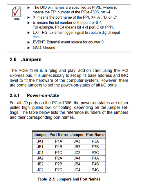
6. Power on state customization: Onboard JP jumper group, each port independently configured with three levels of power on high/low/floating
7. Bus: PCIe x1 PnP, BIOS automatically assigns IRQ and IO base addresses without manual address dialing
8. Transmission performance: Typical IO read/write rate of 1MB/s
Typical Applications
Industrial equipment monitoring and switch control, multi group LED indicator driving, parallel digital data transmission, TTL/DTL/CMOS level signal acquisition, pipeline IO signal detection.
Electrical and Environmental Specifications
|Parameters | Indicators|
|IO level input | High: 2.0~5.25V; Low: 0~0.08V, leakage current -8mA|
|IO level output | minimum high 2.4V, maximum low 0.5V; source 15mA/sink 48mA|
|Working temperature | 0-60 ℃; Storage -20~80 ℃|
|Humidity | 5%~95% No condensation|
|Power consumption | 450mA without peripherals|
|Size | 138.96mm × 98.4mm Half length PCIe Card|
Hardware structure, jumper and terminal definitions
Onboard hardware layout
-JP jumper array: 12 sets of port power level configuration jumpers (JA1/JB1/JC1… JA4/JB4/JC4)
-SW1: Reserved card number dialing (manual not yet enabled)
-CN1:100 pin SCSI-II main IO interface (unique external signal interface)
JP jumper function (port power on status)
Each group of ports corresponds to independent jumpers, with three configurations:
1. Short circuit 1-2: Pull low when powered on (factory default)
2. Short circuit 2-3: Power on and pull high
3. Remove jumper: port floating
Covering all 12 ports A/B/C from P1 to P4.
CN1 100 pin SCSI connector key signal
1. IO signal: P1A0~P4C7, 96 TTL DI/DO channels, divided into three groups of 8-bit A/B/C per PPI
2. Dedicated function pins
-Pin51 EVENT: Counter 0 external pulse input
-Pin99 EXTTRG: External data latch trigger signal
-25/50/75/100: Global signal ground GND
Selection of matching terminal board
1. DIN-100S: Direct connection adapter board, no photoelectric isolation, low-cost universal scenario
2. DIN-96DI: 96 input high-voltage optical isolation terminal board, eliminating ground loop interference
3. DIN-96DO (discontinued EOL): isolated output terminal board
Hardware installation process
1. Anti static operation: Wear an anti-static wristband, touch the chassis to release static electricity, and only hold the edge of the board
2. Jumper pre configuration: Set the power level JP jumper for each port according to device requirements
3. Turn off the power and insert it into any PCIe x1/x4/x8/x16 slot, fix it with screws
4. Connect the 100 core SCSI cable to the matching terminal board
5. Upon startup, the BIOS automatically assigns interrupts and IO base addresses without the need for manual address/IRQ settings
Bottom level register mapping (underlying development core)
The manual fully lists all 32-bit registers offset by base address BASE, core grouping:
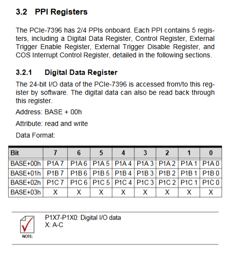
1. PPI data register (BASE+00/10/20/30): reads and writes 24 bit (A/B/C three port) IO data of one PPI, supports output read back
2. PPI control register (BASE+04/14/24/3): Configure A/B/C port input (0)/output (1)
3. External trigger enable/disable register: controls the EXTTRG latch function switch
4. COS interrupt control register: individually enable/disable level jump detection for each group of ports
5. ISC Interrupt Source Control Register (BASE+50): Configure the interrupt trigger source for INT1 and INT2
6. Interrupt clearing register: software clears interrupt flag bit
7. 8254 Timer/Counter Register (BASE40~4C): 3-channel counting channel mode configuration
Hardware working principle
Digital IO and External Trigger Mechanism
-The port can independently input and output; When the external EXTTRG edge arrives, it instantly locks all the current DI states and stores them in the register to avoid software polling loss; The software can configure the triggering edge height to be effective.
8254 timed counting system
-Counter0: External EVENT pulse input, 16 bit countdown, zeroing generates event interrupt
-Timer1+Timer2 cascaded as a 32-bit system timer, onboard 2MHz internal clock, timed overflow output timed interrupt
-All counters support 6 standard 8254 operating modes.
Dual Interrupt System (INT1/INT2)
The board only occupies a single PCIe IRQ in the system, but internally distinguishes between two independent interrupt sources, which are triggered by ISC registers
INT1 optional source
1. P1/P4 all channel COS level change interrupt (default)
2. P1C0/P1C3 pin edge trigger
3. P1C0 falling edge interruption
4. Counter0 count completion event interrupt
INT2 optional source
1. Interruption of COS level changes in all channels of P3/P4 (default)
2. P2C0/P2C3 pin edge trigger
3. P2C0 falling edge interruption
4. 32-bit system timer overflow interrupt
COS level change interrupt
96 inputs, any one of which experiences a high or low voltage jump, and the hardware automatically generates an interrupt request; After the execution of the interrupt service program is completed, write to clear the register and reset the interrupt flag.
Software Support System
1. MAPS Core Basic Driver Kit
-ACE Device Manager: Automatically scan and identify PCIe-7396, configure card number, cache, alias
-Soft panel tool: Visualize read/write IO, test interrupts, trigger functions, no programming or debugging required
2. MAPS/C development library
Windows C/C++DLL library, including initialization, port configuration, IO read/write, trigger, interrupt, timer complete set of APIs, with engineering examples attached
3. MAPS/LV LabVIEW support
Specialized LabVIEW driver library and VI examples for graphical rapid development of automated measurement and control programs