TEWS TVME200 6U VME Bus Industry Pack (IP) Carrier Board
Product Overview
Slot configuration: 4 single size IP module slots; Two dual size IP modules can also be installed. DMA and 32MHz operations are not supported.
address mapping
Mapping the I/O space and ID identification space of IP to VME A16 (short I/O);
Mapping IP memory space to VME A24 (24 bit address) or A32 (32-bit address); Support D08/D16 access;
A24 mode allows for configurable memory size for each IP address; A32 mode occupies a fixed 8 MB per IP.
Interrupt system: Each IP provides 2 interrupts INT0 and INT1; Supports two interrupt configuration methods: ① Rotate switch S3 to select a predefined mapping table; ② The software register can be programmed to map to VME IRQ1-IRQ7 (IRQ7 has the highest priority).
Interface hardware
Four 50 pin flat cable sockets on the front panel, corresponding to IP-A/B/C-D, with all I/O coming from the front;
The 4-pin jumper terminal leads out Strobe gating signals for all IP addresses;
TVME200-20R: IP-D all I/O hard wired to VME-P2; IP-C can route up to 14 I/O channels to the P2 back connector via jumper J3/J4/J5.
Power supply and protection: IP power supply (+5V, ± 12V) with self recovery fuse and RF filter;
LED status indicator light: 4 IP access ACK green lights; +5V (4 channels),+12V, -12V power indicator lights, a total of 10 panel LEDs;
Environment: Working -40 ℃~+85 ℃; Storage -40~+125 ℃; Non condensing humidity 5-95%; MTBF: 366000 hours (MIL-HDBK-217F, 20 ℃ environment); The net weight of the board is 260 grams.
Board no-load power consumption:+5V typical 300 mA,+12V, -12V each 1 mA; actual overall power consumption plus IP module power consumption.
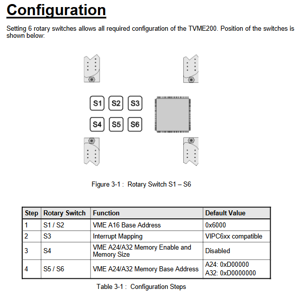
Hardware configuration: 6 rotary dip switches S1-S6
Factory default switch function
S1+S2 VME A16 base address 0x6000 (S1=6, S2=0)
S3 Interrupt Mapping Mode 1 (compatible with VIPC6xx)
S4 A24/A32 memory enabled+single IP memory size 0 (memory disabled)
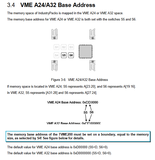
S5+S6 VME A24/A32 memory base address A24:0xD00000; A32:0xD0000000
2.1 VME A16 Short I/O Address (S1, S2)
The carrier board occupies a total of 1 KB of A16 space; each IP is allocated 256 bytes.
S3=0-7: Each IP: 128B I/O space+64B ID space+64B IRQ&control registers; Software configurable interrupt and IP reset.
S3=8-F: IRQ and control registers are inaccessible; The original register of 64 bytes is merged into the ID space, which is expanded to 128 bytes for IP modules that require large ID-PROM.
Default base address 0x6000: IP-A: 0x6000; IP‑B:0x6100; IP‑C:0x6200; IP‑D:0x6300。
2.2 Interrupt Configuration S3
S3 value 0-7: Both hardware predefined interrupt mapping and software IRQ configuration register are enabled, and software can rewrite interrupt routing;
S3 value 8-F: The same set of predefined interrupt mappings, but software registers are closed and cannot be programmed to modify interrupts.
S3=1 is the factory default and compatible with VIPC6xx; S3=2 compatible with VIPC610-01; S3=3 compatible with VIPC310. Each IP has two interrupts, INT0 and INT1, which can be mapped to VME IRQ1~IRQ7 or configured to disable interrupts.
2.3 A24/A32 Memory Settings S4
S4=0: Memory function turned off.
A24 mode (S4=1-7): Single IP memory: 32K~2 MByte; The memory size of all four IPs is the same, and the S4 gear is set based on the maximum IP requirement;
S4=F: Enable A32 mode; Each IP is fixed at 8 MB, for a total of 32 MB.
2.4 A24/A32 base addresses S5, S6
The memory base address must be aligned with the memory size boundary selected by S4.
A24: S5 sets A [23:20], S6 sets A [19:16];
A32: S5 sets A [31:28], S6 sets A [27:24].
Register definition (S3 must be accessible from 0-7)
All registers are located in the VME-A16 address space, with one set for each IP: IRQ configuration register and Control control register.
3.1 IP IRQ Configuration Register
Select the VME interrupt level for INT0 and INT1 of each IP using 3 bits respectively; 000 represents the interruption of closing the circuit; 001-111 corresponds to IRQ1-IRQ7; The power on reset value is determined by the S3 hardware switch.
3.2 IP Control Register
Bit function for reading and writing
Bit7 IP reset: Writing 1 triggers IP reset; Hardware auto reset; Readable reset status R/W
Bit2 Error # Signal Status (IP Module Error) R
Bit1 INT1 interrupt hanging flag R
Bit0 INT0 interrupt hanging flag R
Bit6-3 reserved bit, read as an indefinite value R
This register allows software to reset IP, read interrupt suspension status, and read IP module error signals.
Strobe gating signal
The Strobe # signal of the IP logic interface is led to the 4-pin jumper block of the board for all four IPs; Can be used as an input or output of an IP module for clock/trigger gating.
Precautions for IP module installation
Power off operation; IP belongs to ESD static sensitive devices, wear anti-static wristbands and anti-static pads;
The IP slot has error prevention keys and can only be inserted in one direction;
In high vibration and impact environments, the IP module needs to be locked with the TIPxxx-HK screw washer kit;
Front panel 50 pin flat cable, connector with lock buckle, cable pin 1 marked.
Panel LED Description
ACK (green): When accessing the corresponding IP, it lights up for about 200ms; A/B/C/D correspond to 4 slots respectively;
Power LED (green):
+5V A/B/C/D: The 5V power supply for each IP slot is normal;
+12V, -12V: A positive and negative 12V power supply shared by all IPs.
All IP power circuits use self recovering fuses, plus RF filtering.
TVME200-20R Back I/O Characteristics
10R version P2 has no user I/O; The 20R supports back I/O.
All 50 I/O hard wired connections of IP-D are simultaneously connected to the front panel 50 pin socket and VME-P2 connector A/C row; If the backplane P2 is occupied by other functions, the D slot cannot use IP modules with I/O;
IP-C: All 50 I/O channels are connected to J3 jumper socket; Up to 14 signals can be connected to VME-P2 via J4/J5 jumpers; By default, the back is not connected at the factory;
Manual reminder: When back I/O is not required, TVME200-10R is preferred for better signal isolation and integrity.
Pin allocation
IP-J1 logical interface: 50pin, VITA4 standard IP bus signal (data D0-D15, addresses A1-A6, Reset #, IntReq0 #/1 #, Error #, Strobe #, DMA signal, power+5V/+12V/-12V, GND, etc.); This carrier board does not implement DMA related signals.
IP-J2 I/O interface: Customized I/O for IP modules, directly connected to a 50 pin flat cable socket on the front panel.
VME P1 complete VME bus signal;
The P2 of TVME200-10R is basically empty, only the high bit address of VME;
TVME200-20R P2: A/C row allocates all IP-D I/O; Some pins can be connected to 14 I/O channels of IP-C through jumper wires.
Key Limitations
Not supporting DMA and 32MHz transmission; Only supports D08/D16;
Four IPs in A24 mode must have the same memory size set, and S4 should be set according to the maximum requirement;
A24/A32 memory base addresses must have boundary alignment;
Software programmable interrupt and reset registers only take effect when S3=0-7; S3 ≥ 8 can only be mapped using hardware predefined interrupts;
When TVME200-20R uses D-slot IP, the A/C row of VME chassis P2 cannot be allocated to other cards;
The installation of IP modules must be anti-static and plug and unplug when powered off.