NI CompactRIO Embedded System
The official user manual for NI CompactRIO Embedded System 2025 covers the complete software and hardware configuration of CompactRIO controllers, chassis, Single Board RIO, myRIO, and C Series I/O modules. The core includes compatibility between driver versions and LabVIEW, three programming modes (Scan Interface/FPGA Interface/Hybrid), project construction, module configuration, multi module synchronization, temperature/LED/sleep/reset control, data read/write and calibration, troubleshooting, and supports all types of analog/digital/counter/motion/CAN/serial I/O. It is an authoritative guide for developing high-performance measurement and control systems based on LabVIEW FPGA/Real Time.
CompactRIO System Architecture
Standard components: real-time processor+reconfigurable FPGA+C Series I/O module
Topology: FPGA connects modules in a star pattern to achieve precise timing and synchronization.
Product Form:
CompactRIO controller (cRIO-903x/904x/905x/906x)
Single‑Board RIO(sbRIO)
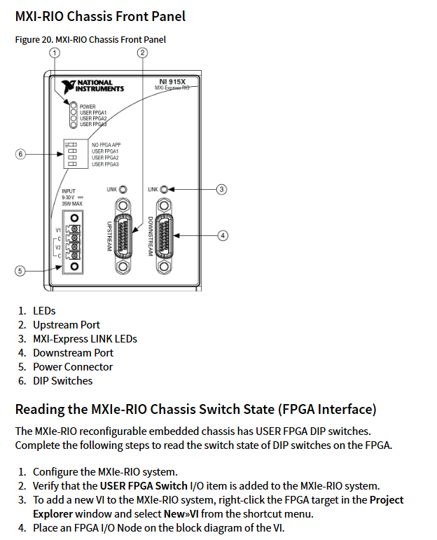
Ethernet RIO/MXIe-RIO chassis
myRIO、roboRIO、NI ELVIS RIO CM
Three programming modes
Mode Characteristics Applicable Scenarios
Scan Interface does not require FPGA programming, I/O variables, automatic scanning for fast development, universal acquisition, and simple control
FPGA Interface custom VI, highest precision, synchronous, parallel high-speed acquisition PWM、 Encoder, hard real-time
Hybrid module Scan and FPGA hybrid requirements: high-speed+universal acquisition
LabVIEW project configuration process
Online configuration
Create a new project → Discover hardware → Select programming mode → Automatically identify modules → Deploy.
offline configuration
Manually add controller → chassis → FPGA Target → add C Series module.
CRIO-904x/905x enhancement
Support dynamic switching between Real Time Mode/Scan Mode/FPGA Mode.
Native support for NI DAQmx.
Core I/O configuration (digital+analog)
1. Advanced digital I/O functions
Supported configurations include: counter, frequency/cycle measurement PWM、 Orthogonal encoding input.
Filter mode: Disabled/1 µ s/16 µ s/256 µ s/4096 µ s.
Counter mode:
edge count
Periodic measurement
Pulse width measurement
frequency measurement
2. Analog configuration
Support: calibration conversion, range setting, synchronous sampling, disconnection/over limit detection.
Core formula:
Engineering unit=(binary value x LSB weight) – offset
Synchronization rules:
Unified master clock source
Simultaneously start
Read from the same FPGA I/O node
Advanced System Control
Sleep mode
Module enters low power consumption, communication returns error.
System Reset
Software reset the entire machine, FPGA cleared, and output restored to power on state.
FPGA LED
Programmable on/off, used for status indication.
temperature reading
Temperature=binary value x 0.25 ℃.
Multi module synchronization
Synchronize with the same chassis
Set a module as Master and export clock
Set the rest as Slave and import the clock
Simultaneously start and unify FPGA I/O node reading
Cross chassis synchronization
Using NI 9469 time synchronization module
Export clock from main NI 9469, import from module
Overview of Hardware Models
1. Controller series
Characteristics of Series CPU FPGA
CRIO-903x dual core/quad core Kintex-7 wide temperature WiFi、 4/8 slots
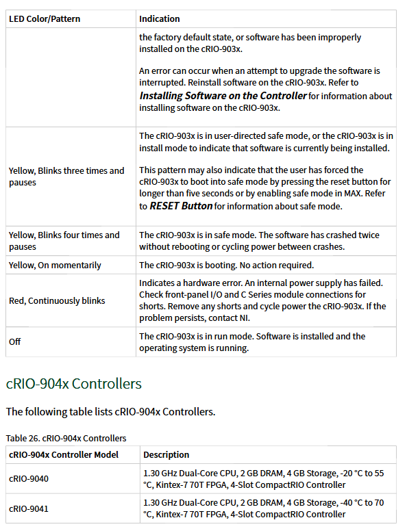
CRIO-904x dual core/quad core Kintex-7 extreme wide temperature range (-40~70 ℃)
CRIO-905x Dual Core Artix-7 High Cost Performance
CRIO-906x 667MHz Zynq-7020 Classic Low Power Consumption
2. C Series module categories
AI: Voltage/Current/Vibration/Strain/Temperature (NI 92xx)
AO: Voltage/Current Output (NI 926x)
DIO: High Speed/Isolation/High Power (NI 94xx)
Counter:NI 932x
Sports: NI 950x
CAN:NI 9852/9853
Serial port: NI 987x
Synchronization: NI 9469
Key issues
Question 1: What is the core difference between Scan Interface and FPGA Interface? What projects are suitable for each?
answer:
Scan Interface: No need to write FPGA VI, the system automatically scans I/O, the fastest development, but the synchronization accuracy and speed are limited; Suitable for rapid development, universal collection, and simple logic control.
FPGA Interface: Custom logic needs to be written using LabVIEW FPGA modules, which can achieve microsecond level synchronization, high-speed pulses, encoders, and parallel processing; Suitable for professional measurement and control systems with high precision, high real-time, and multi-channel synchronization.
Question 2: How can multiple C Series analog modules achieve strict synchronous acquisition?
answer:
Set one of the modules as Master and enable ‘Export Onboard Clock’.
The remaining modules are set as Slave, with the clock source pointing to the main module.
All modules trigger Start simultaneously.
Use the same FPGA I/O node to read all channels, ensuring that the sampling time is completely consistent.
Question 3: What are the unique advantages of cRIO-904x/905x compared to other controllers?
answer:
Supports dynamic switching between three programming modes (Real Time/Scan/FPGA).
Native support for NI DAQmx, can be used like a data acquisition card.
Featuring a wider temperature range (-40~70 ℃) and stronger anti-interference design.
Supports high expansion interfaces such as USB-C, dual Ethernet, real-time clock, hardware latch triggering, etc.