ADLINK DAQ -/DAQE -/PXI-2000 Series Multi functional Synchronous Acquisition Card
Product Overview (Features, Specifications, Software Support)
1.1 Core Hardware Features
1. Analog input AI (4-channel differential synchronous acquisition, standard across the entire series)
|Model | Resolution | Maximum Sampling Rate | On Chip FIFO|
|2010 | 14 bit lossless code | 2MS/s | 8K sampling points|
|2016 | 16 bit lossless code | 800kS/s | 512 sampling points|
|2005 | 16 bit lossless code | 500kS/s | 512 sampling points|
|2006 | 16 bit lossless code | 250kS/s | 512 sampling points|
-Programmable gain: × 1/× 2/× 4/× 8; The input range is divided into bipolar (± 10/± 5/± 2.5/± 1.25V) and unipolar (0~10/5/2.5/1.25V); Common mode voltage ± 11V, power on withstand voltage ± 30V, power-off ± 15V, input impedance 1G Ω/100pF.
-Performance indicators: Provide -3dB small signal bandwidth, system noise (LSBrms), DC~60Hz common mode rejection ratio CMRR table; Built in 40MHz internal time base, supporting 1-40MHz external clock.
-Transmission method: software polling, distributed/aggregated bus master control DMA; Four triggering modes: pre triggering, post triggering, delayed triggering, and intermediate triggering; Support software/external simulation/external digital/SSI synchronous trigger source.
2. Analog output AO (2-channel 12 bit voltage output, universal across the entire system)
-Maximum update rate 1MS/s; Single channel FIFO 2K, dual channel 1K; output range can be selected from internal 10V reference or external AOEXTREF.
-Electrical specifications: establishment time of 3 μ s (0.5LSB), slew rate of 20V/μ S, output impedance of 0.3 Ω, maximum driving ± 5mA, short circuit protection; The factory has zero bias and large gain error, and the accuracy is greatly improved after automatic calibration.
-Output mode: software instant update, timed waveform generation (limited/infinite iteration, re triggering, waveform interval delay DLY2), with 3 shutdown modes available.
3. Digital IO and synchronous digital input SDI
-Universal GPIO: 24 channel 82C55A TTL/CMOS programmable IO, default high impedance input when powered on; Divided into PA/PB/PC three 8-bit ports, high and low byte can be independently configured for input and output.
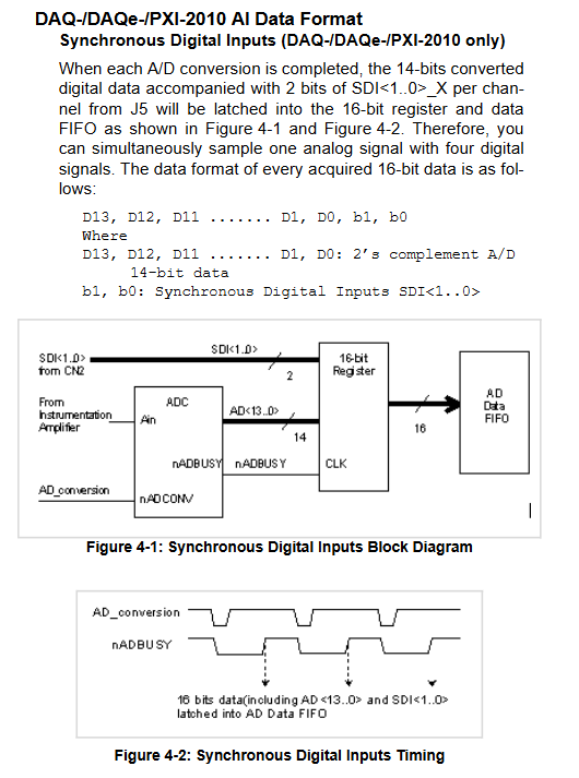
-SDI is only unique to the 2010 model: 8-channel synchronous digital input, synchronized sampling with analog signals, data packaged and stored in the lower 2 bits of 16 bit AI data.
4. Universal Timer Counter GPTC
-Two independent 16 bit up/down counters, with a maximum external clock of 10MHz; 8 working modes: counting, cycle measurement, pulse width measurement, single pulse/continuous pulse generation, gate pulse, etc; Clock, gate control, increase/decrease direction, and output polarity software are programmable.
5. Synchronous interface SSI
-DAQ models come with a 20 pin SSI synchronous ribbon interface, while PXI models reuse the backplane PXI trigger bus; 6-way bidirectional synchronous timing signal, supporting one master, multiple slaves, and multi card synchronization to achieve multi card synchronous acquisition/output.
6. Simulate triggering, physical and environmental parameters
-Simulation trigger: can choose any AI channel or external analog input of EXTATRIG, 8-bit trigger level, 5 trigger judgments (below threshold, above threshold, within interval, high latency, low latency); External digital triggers include A/D specific EXTDTRIG and D/A specific EXTWFTRIG, TTL level, with a minimum pulse width of 10ns.
-Physical dimensions: DAQ/DAQE board size 175 × 107mm, PXI standard CompactPCI size; The main I/O is a 68 pin VHDCI interface.
-Power supply, temperature and humidity: Provide typical power consumption of+5V,+12V, and+3.3V for each model; Working at 0-55 ℃, storage at -20~80 ℃, humidity at 10%~90% without condensation.
1.2 Typical application scenarios
Automotive testing, cable inspection, transient signal measurement, automated testing equipment ATE, laboratory automation, biomedical signal acquisition.
1.3 Full stack software support (included with accompanying CD)
1. Bottom level development libraries
-D2K-DASK: Windows DLL driver, supports VB/VC+/Delphi, etc;
-D2K-DASK/X: Linux shared library, developed with GCC.
2. Industrial control upper driver
-DAQ-LabVIEW PnP: Free LabVIEW driver VI library, no authorization restrictions;
-D2K-OCX: ActiveX control, suitable for rapid development of interfaces in VB/VC.
3. Visualization tool DAQPench: ActiveX measurement control suite, available for free 4-hour trial, commercial use requires separate authorization.
4. All driver manuals are stored on a CD and can only run a 2-hour demo version without authorization.
Hardware Installation Guide
2.1 Packaging List
Collecting card body, integrated driver CD, software installation manual; Missing/damaged items require contacting the dealer and retaining the packaging for easy storage and repair.
2.2 Anti static operation specifications
The board contains static sensitive chips and must be operated with a grounded anti-static pad and an anti-static wristband; After unboxing, check the circuit board for any transportation damage and press the patch IC to ensure proper adhesion; Damaged boards are strictly prohibited from being powered on.
2.3 Board Layout Differentiation
1. DACe (PCIe): Only 68 pin VHDCI main interface, without SSI cable socket;
2. DAQ (PCI): 68 pin main interface+20 pin SSI synchronous interface J3;
3. PXI: No external SSI cables, timing synchronization relies on the PXI backplane P2 bus.
2.4 PCI Plug and Play Configuration
The entire board has no jumpers, IRQ、DMA、 The base address is automatically assigned by BIOS and does not require manual setting; Provide PCI_SCAN tool to read hardware resources; Most faults are interrupt conflicts, and it is necessary to enter BIOS to adjust hardware interrupt allocation.
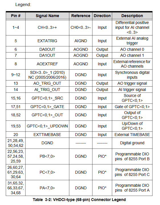
Definition of Signal Wiring and Analog Input Wiring Scheme
4.1 Definition of connector pins
1.68-pin VHDCI main interface
-AI differential channel: CHO~CH3+/-; Simulate triggering EXTATRIG and simulating ground AIGND;
-AO channel DA0/DA1OUT, external reference AOEXTREF, analog ground AOGND;
-Digital trigger: EXTDTRIG (A/D), EXTWFTRG (D/A);
-Timer: GPTC0/1 clock, gate control, direction, output; External time base EXTTIMEBASE;
-Auxiliary timing AFI0/AFI1, synchronous digital SDI (2010 only); AI/AO triggers the output of AI \ _Trig_out, AO \ _Trig_out;
-24 GPIO PA/PB/PC ports, digital ground DGND.
2.20-pin SSI synchronous interface (DAQ series)
contain SSI\_TIMEBASE、SSI\_ADCONV、SSI\_SCAN\_START、SSI\_AD\_TRIG、SSI\_DAWR、SSI\_DA\_TRIG Six bidirectional synchronous clock/trigger signals, with the remaining pins grounded or reserved.
4.2 Two wiring methods for analog input
1. Single ended input: All negative terminals of the channels are uniformly connected to AIGND, with simple wiring but poor anti-interference, only for easy measurement and use;
2. Differential input (recommended): Suppress common mode noise, divided into two types of signal sources:
-Grounding reference source: direct CHn+signal connection, CHn – signal grounding;
-Floating signal source (thermocouple, isolated output): A bias resistor needs to be added to provide a return path to avoid input floating drift.
Working Principle (Core Function Timing, Mode, Transmission)
4.1 A/D modulus acquisition principle
1. Data encoding format
-2010 (14 bits): Supplement format, storing SDI synchronized digits in the lower 2 bits of 16 bit data;
-2005/2006/2016 (16 bit): Direct binary encoding, divided into single/bipolar code value comparison table.
2. Two collection modes
-Software polling: Single trigger conversion, software reading, sampling timing controlled by the program, unstable rate;
-Programmable scanning acquisition (high-precision recommendation): Set the scanning interval for the SI counter and the total number of samples after triggering the PSC counter; 40MHz internal time base calculation sampling period, synchronous sampling of 4 channels simultaneously, scanning interval=sampling interval.
3. Four major triggering acquisition timing sequences
-Pre trigger: Save M sets of scan data before triggering; M \ _denable can forcibly fill M sets of data before responding to trigger;
-Post trigger: Only collect PSC group data after triggering; Support re triggering, multiple triggers for segmented storage;
-Intermediate trigger: Simultaneously save M sets of data before triggering and N sets of data after triggering;
-Delay trigger: After triggering, wait for the Delay \ _comounter count to complete before starting the collection.
4. DMA distributed/aggregated transmission
PCI bus controls DMA without the need for CPU to transfer data; Support non contiguous memory linked lists (scatter/path) with no upper limit for single transfer; Circular linked list can achieve multi buffer continuous acquisition and reduce CPU load.
4.2 Principle of D/A Digital Analog Output
1. The reference source can be selected as internal 10V or external AOEXTREF, with output voltage=digital code x reference voltage, supporting amplitude modulation (external AC reference); Provide a comparison table of single/bipolar code values.
2. Output mode:
-Software instant update: Single output fixed voltage, suitable for static level;
-Timing waveform generation: UI counter output update interval, UC single waveform point count, IC iteration count, DLY1 trigger delay, DLY2 waveform interval; Supports limited/infinite waveforms and re triggering.
3. Three shutdown modes: immediate stop, complete current waveform stop, complete integer round iteration and then stop.
4.3 Digital IO
24 channels of 82C55A general-purpose GPIO, with independent input and output configuration for high and low ports of 4 bits; 2010 unique SDI synchronous digital input, synchronized with analog sampling for locking.
4.4 GPTC Timer 8 Working Modes
Gate control counting, cycle measurement, pulse width measurement, gate control single pulse, trigger single pulse, re trigger single pulse, single trigger continuous pulse, gate control continuous pulse; All counting parameters and signal polarity software configurations.
4.5 All types of trigger sources
1. Software triggering: No external circuit is required, function calls can directly start collection/output;
2. External simulation trigger: EXTATRIG or AI channel signal, 5 threshold judgments;
3. External digital trigger: EXTDTRIG (A/D), EXTWFTRG (D/A), with selectable rising/falling edges;
4. SSI bus trigger: Multi card synchronous shared clock and trigger signal.
4.6 User controllable timing signals and multi card synchronization
1. Classification of timing signals: internal timing of the board (time base, AD conversion, scan start, DA update, etc.), AFI external auxiliary input, AI/AO trigger output, SSI synchronization bus;
2. AFI multifunctional input: AFI0 replaces external ADCONV/SCAN \ _stART, AFI1 replaces external DAWR;
3. SSI master-slave synchronization: Single signal, one master, multiple slaves, clock, trigger, and conversion signals are synchronized across cards to achieve 4 × N channel synchronous acquisition; The PXI model reuses the backplane trigger bus without the need for wiring.
Calibration Function (Ensuring Acquisition/Output Accuracy)
1. Calibration constant storage: The factory calibration parameters are fixed in the onboard EEPROM and automatically loaded into TrimDAC when powered on; EEPROM distinguishes between factory default area and user-defined storage area, and can store multiple sets of calibration parameters.
2. Automatic calibration of Auto library
-No external standard source required, relying on onboard 5V high-precision reference source (temperature drift ± 2ppm/℃);
-Pre requirements: Preheat the board for 15 minutes and remove external wiring; Automatically correct zero offset and gain error; After calibration, the offset error is ≤ ± 1mV, and the gain error is significantly reduced.
3. Save calibration parameters: After automatic calibration is completed, new parameters can be stored in the EEPROM user partition, with calibration time and temperature records, and can be switched and called in multiple environments.