SIEMENS C500 microcontroller family architecture and instruction set description
Infrastructure
compatibility
The C500 family is fully compatible with the standard 8051 microcontroller architecture and software, and is up compatible with SAB 80C52/80C32.
Storage Architecture (Harvard Architecture)
|Storage Type | Location | Capacity Range|
|Program Memory | Internal | 2KB~64KB|
|Program Memory | External | Maximum 64KB|
|Data Storage | Internal | 128B/256B|
|Data Storage | XRAM | 256B~3KB|
|Data Storage | External | Maximum 64KB|
|Special Function Register SFR | Internal | 128B Standard+128B Mapping|
Internal data storage partition
Low 128B (00H~7FH): Directly/indirectly addressable, including 4 sets of general-purpose registers and a 128 bit addressable area.
High 128B (80H~FFH): Only indirectly addressed.
SFR area (80H~FFH): Only direct addressing, partially supports bit operations.
CPU architecture
Core register
ACC (accumulator A): Data operation core.
B Register: Dedicated for multiplication and division.
PSW (Program Status Word): Contains flag bits such as carry, auxiliary carry, overflow, register group selection, etc.
SP (stack pointer): 8-bit, reset to default 07H.
Data pointer DPTR: Standard 1, C500 supports 8, selected through DPSEL.
Core strengths
8 sets of data pointers: external memory access speed is increased by about 1 times, saving memory and instructions.
Enhanced Hook Simulation: No bond out chip required, supports on-chip ROM program simulation.
interrupt system
The vector address has a fixed interval of 8 bytes, starting from 0003H.
Response time: minimum 3 machine cycles, maximum 9 machine cycles.
CPU timing
1 machine cycle=6 states (S1~S6), each state divided into P1/P2 phases.
Instruction cycle:
Most instructions: 1 cycle.
Multiplication and division instruction (MUL/DIV): 4 cycles.
External access instruction (MOVX): 2 cycles.
Instruction set
Basic Parameters
Total number of instructions: 111.
Single byte: 49 entries; Double byte: 45 entries; Three bytes: 17 entries.
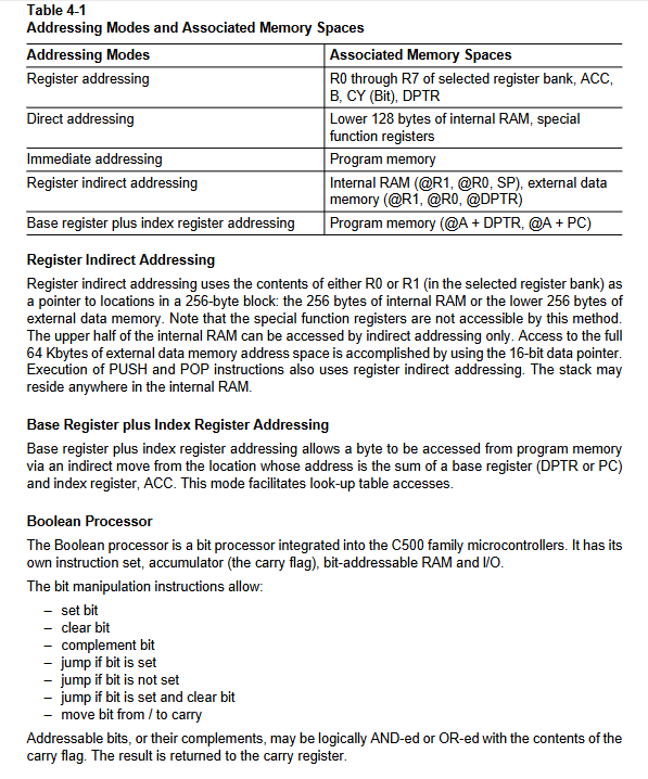
Addressing methods (5 types)
Register addressing, direct addressing, immediate addressing, register indirect addressing, base address+index addressing.
command classification
Data transmission: MOV, MOVX, MOVC, PUSH/POP, XCH.
Arithmetic operations: ADD, ADDC, SUBB, MUL, DIV, DA, INC/DEC.
Logical operations: ANL, ORL, XRL, CLR, SETB, CPL, shift.
Control transfer: AJMP/LJMP/SJMP, ACALL/LCALL, RET/RETI, conditional jump.
Operational ability
Built in Boolean processor, supporting bit reset, inversion, jump, and AND/OR operations.
Encapsulation information
Provide three mainstream packaging options, covering both direct insertion and surface mount scenarios:
P-DIP: 40 pin direct insertion.
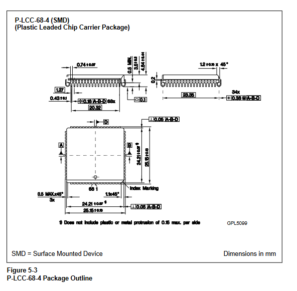
PLCC: 44/68/84 pin patch.
MQFP: 44/80/100 pin square patch.
Key issues
Question 1: What is the most essential hardware enhancement of C500 compared to standard 8051? What value does it have?
Answer: The core enhancement is to support up to 8 sets of 16 bit data pointers (DPTR0~DPTR7), which can be switched through DPSEL registers. Value: The external memory access speed is increased by about 1 times, reducing the number of instructions and internal RAM usage, making it more suitable for high-level languages and high-capacity peripheral access.
Question 2: What are the instruction set size and addressing method of C500?
Answer: The instruction set consists of 111 instructions, including 49 single byte, 45 double byte, and 17 three byte instructions; Supports 5 addressing methods: register addressing, direct addressing, immediate addressing, register indirect addressing, and base address+index addressing.
Question 3: What is the interrupt response time of C500? What factors affect it?
Answer: The minimum interrupt response time is 3 machine cycles, and the maximum is 9 machine cycles. Influencing factors: higher priority interrupt being executed, current instruction not completed, current instruction being RETI or interrupt register write operation.