ADLINK ACL-7122 144 bit digital I/O board
Chapter 1 Product Overview (Introduction)
1.1 Core functional characteristics
I/O channel: Standard 144 TTL/DTL compatible digital input/output, switchable to 96 channel mode via jumper
Chip architecture: Simulate 6 Intel 8255 PPI chips (only Mode 0 basic input-output mode)
Drive capability: onboard buffer circuit enhances output drive; Support output status readback
Interrupt function: Programmable hardware edge interrupt, multiple cards can share the same IRQ interrupt line
Physical specifications: Half length ISA card, size 183mm × 111mm, suitable for various industrial control chassis
Expansion adaptation: Directly connect to OPTO-22 isolation terminal board
1.2 Typical application scenarios
Industrial equipment switch monitoring, digital control of relays/solenoid valves, key/contact signal acquisition, combined with AD/DA modules to form a complete data acquisition and control system.
1.3 Electrical specifications
Enter electrical parameters
High level: 2.0~5.25V, input current 22 μ A
Low level: 0~0.8V, injected current -0.2mA
Output electrical parameters
PA/PB port: High level ≥ 2.4V (pulling current -2.6mA); Low level ≤ 0.5V (fill current 24mA)
PC port: 5V power supply, typical 1.4A, maximum 1.8A
Transmission and Performance
Typical transmission rate of 300KB/s, up to 500KB/s
Signal level standard TTL 5V
Chapter 2 Hardware Installation
2.1 Anti static code for unpacking
The board contains precision ICs and requires anti-static pads and wristbands throughout the entire process; Before receiving the goods, check for transportation damage and reinforce all socket ICs by pressing them; Damaged boards are prohibited from being powered on.
2.2 Definition of Board Jumper and DIP Switch
JP7 (Channel Mode Switching)
Default 144 bit mode: occupying 32 consecutive I/O addresses, with a minimum interval of 8 between single card addresses;
96 bit mode: occupying only 16 I/O addresses, multiple cards can be arranged continuously;
SW1 (5-digit dialing, base address setting)
Base address range: 0x200~0x3FF; A9 is fixed at 1, while A3~A0 hardware forces 0, only adjusting A8~A4;
Rule: Dial ON=0, OFF=1, the manual provides typical address configuration examples such as 0x2C0;
JP6 (IRQ Interrupt Selection)
Supports 11 levels of interrupts for IRQ3/4/5/6/7/9/10/11/12/14/15; Default IRQ15;
Interrupt signal tri state output, multiple ACL-7122 can share the same IRQ;
JP0~JP5 (6 independent interrupt enabled channels)
Three levels for each jumper:
D: Interrupt disabled;
E: Hardware edge triggered interrupts (rising edge of PC0, falling edge of PC3);
P: Programmable interrupt (triggered when PC4 is set low);
Interrupts only capture edges, without signal locking, and cannot distinguish the triggering channels in sequence.
2.3 Definition of connector pins
The board is equipped with 6 50 pin IDC sockets, each corresponding to one 8255 (CH0~CH5), with single channel pin allocation:
1-24 pins: Port C (8 bits), Port B (8 bits), Port A (8 bits)
49/50 pins:+5V power supply; All even pins are grounded
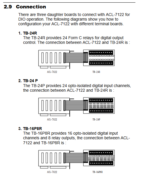
2.4 Matching Terminal Board Wiring Scheme
Supports 3 types of OPTO-22 compatible terminal boards:
TB-24R: 24 way relay output terminal board
TB-24P: 24 channel optocoupler isolation input terminal board
TB-16P8R: 16 isolated inputs+8 relay hybrid terminal board
Chapter 3: Digital I/O Programming
3.1 I/O Register Address Mapping (Default Base Address 0x2C0)
Six 8255 channels, each occupying four consecutive addresses (PA data, PB data, PC data, control word), totaling 24 valid register addresses. The remaining reserved addresses for the remaining modes are not used.
3.2 8255 Mode 0 Operating Logic
PA, PB: independent 8-bit bidirectional ports; PC is divided into two groups of 4-bit ports: upper 4-bit and lower 4-bit
16 input/output combination configurations, defined by control words D0~D4 bits;
Output port data latch, input port no latch; Can read the current state of the output register.
PC0 and PC3 can be used as hardware interrupt edge inputs.
3.3 Complete Interrupt Logic
E (hardware triggered) mode: PC0 rising edge/PC3 falling edge triggers interrupt;
P (Programmable) mode: PC4 must be pulled low to respond to PC0/PC3 edges; PC4 high-level shielding interrupt;
Software self-test: It can output level simulated external interrupt signals to the PC port for program debugging.
3.4 Key considerations for programming
After power on/reset, all ports default to input mode and output buffer high resistance;
After switching the output mode, a write operation must be performed once to output the voltage level;
The power on output latch value is random, and the program must initialize the port level before starting;
When the port is set to output, it can read back the output data of the latch.
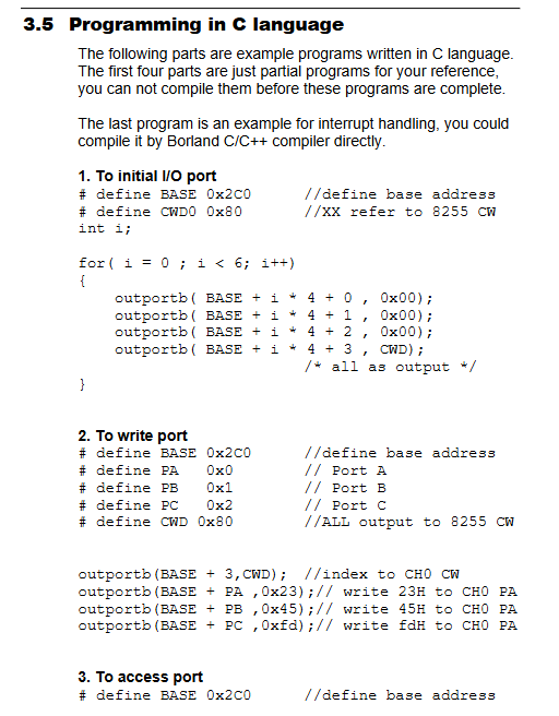
3.5 C language complete example code
Provide 5 directly compiled routines for Borland C:
Initialize all ports of 6 channels (set as output);
PA/PB/PC port data writing;
Read the input status of the port;
Interrupt clearing and enabling operations;
Complete interrupt service program (IRQ9 test, key triggered buzzer alarm), including interrupt vector save/restore, 8259 interrupt EOI instruction.
Appendix A: PC Standard I/O Port Address Mapping
List the I/O addresses occupied by native hardware on the PC motherboard (serial port, parallel port, floppy drive, graphics card, game port, etc.) to avoid ACL-7122 base address conflicts.