ADLINK 743X series isolated digital IO board
Basic Information
ADLINK NuDAQ/NuIPC 743X series PCI/cPCI isolated digital IO card, including PCI standard PCIe board, 3U CompactPCI front IO, rear R IO multiple versions
Product line classification
PCI Short Card: PCI-7432 (32DI+32DO), PCI-7433 (64DI), PCI-7434 (64DO)
CPCI standard prerequisites: cPCI-7432, cPCI-7433, cPCI-7434
CPCI Rear IO Version: R Basic Version, RP Common Power Version (cPCI-7432R/RP, 7433R, 7434R/RP)
The core commonality is that the entire system adopts PLX PCI-9050 PnP controller, which supports BIOS automatic allocation of interrupt/IO addresses; Optocoupler electrical isolation, with a maximum isolation voltage of 5000Vrms; Unified 100Pin SCSI-II external interface, with a maximum read and write speed of 10kHz.
Core functions and specifications of the product
1. Summary Table of Hardware Channels and Isolation Differences for Various Models
Model: DI Channel, DO Channel, Isolation, Voltage Resistant Output Driver, Special Configuration
PCI-7432/cPCI-7432 32 isolated input 32 isolated output 5000Vrms single channel maximum 500mA current DI0/1 dual channel hardware interrupt
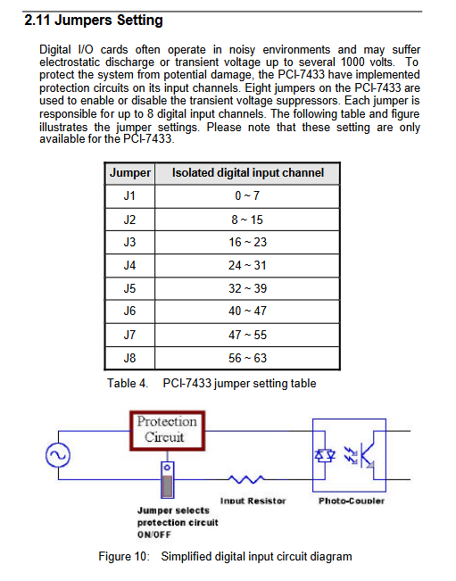
PCI-7433/cPCI-7433 64 isolated input no output 2500Vrms -8 sets of input surge protection jumpers, supporting 50V input
PCI-7434/cPCI-7434 no input 64 isolated output 5000Vrms single channel maximum 500mA divided into 8 groups output common power VDD
The R/RP rear series channel corresponds to the standard version channel, and the R version 2500V output has two types of wiring: common ground/common power. The cPCI backplane J2 rear signal
2 Digital Input Electrical Specification (IDI)
Logic level: High 5~24V, Low 0~1.5V; PCI-7433 supports up to 50V input
Input internal resistance: 7432 is 2.4K Ω, 7433 is 4.7K Ω
Isolation: Optocoupler isolation, supporting both source and drain external sensor wiring
Interrupt: 7432/7433 Only DI0 and DI1 can trigger hardware interrupts
Bandwidth: up to 10kHz acquisition rate
Protection: PCI-7433 board with 8 sets of jumper wires, each set controls the on/off of 8-channel transient suppression protection circuit
3 Digital Output Electrical Specification (IDO)
Output chip: ULN2803 Darlington transistor drain output
Load range: External 5~35VDC; Single channel continuous 500mA, total power consumption of 2.25W per chip
Grouping design: Every 8 outputs share a set of VDD common power supply and IGND return ground; RP version unified common power architecture
Inductive load requirements: Relays/coils must be connected in parallel with freewheeling diodes to suppress reverse high-voltage breakdown of the chip
Onboard auxiliary power supply: Each connector leads out a V5V onboard non regulated 5V output
4 General Machinery and Environment
PCI card size: 173mm long x 106mm high standard short PCI board
CPCI Full Series: Standard 3U Industrial Control Board Size
Working temperature: 0-60 ℃; Storage -20~80 ℃; Humidity 5%~95%, no condensation
Power consumption: 7432 typical+5V 530mA; 7433 typical+5V 500mA; 7434 typical+560mA
Hardware structure, connector and jumper specifications
1. PCB layout differentiation
PCI-743X: Only front 100Pin CN1 SCSI interface, no backplane J2
CPCI Standard Edition: Front CN1, side reserved cPCI J2 backplane pin (no rear IO)
CPCI-R Rear Series: CN1 is a rear adapter board output, and the chassis backplane J2 transmits IO signals, which must be used with a DB-100RU rear transition board
The document is accompanied by three board layout drawings, indicating the PCI controller and CN1/J2 positions.
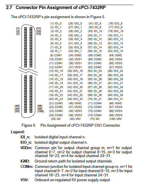
2 100Pin SCSI-II connector pin rules
Universal Pin Definition Identification:
IDI-n: nth isolated digital input
IDO-n: nth isolated digital output
COMm: Each group has 8 DI common terminals (can be connected to 24V or GND, compatible with source/drain sensors)
VDDm: Each group has 8 channels of DO external power supply common positive pole
IGND: Output circuit return ground
V5V: Onboard 5V auxiliary power supply
List of independent pins by model: 7432, 7433 PCI-7434、cPCI-7434R/RP, Distinguish between the definitions of common ground and common power output wiring.
3 jumper configuration (PCI-7433 only)
There are a total of 8 sets of jumper wires on board J1-J8, each corresponding to 8 DI channels. Short circuiting enables transient voltage suppression protection, disconnecting and disabling the protection circuit. The physical location of the jumper wires and the simplified input circuit are marked on the drawing.
4 Input/Output Standard Wiring Schematic Diagram
Isolation input with two connection methods: source type (COM connected to 24V) and drain type (COM connected to GND), with accompanying optocoupler and current limiting resistor circuit schematic diagram
Output two types of wiring:
Common ground R version: load negative terminal connected to IGND, VDD connected to external 24V positive terminal
Common Power RP Version: The positive pole of the load is uniformly connected to VDD, and the negative pole is connected to IGND, suitable for batch solenoid valve drive
Register low-level definition (aimed at low-level developers)
PCI configuration area: PCI-9050 bridge chip registers, BIOS automatically assigns base addresses and interrupts, manual modification is prohibited to avoid resource conflicts
The local IO register has a uniform 32-bit width and only supports 32-bit read and write operations. Accessing 8/16 bits will result in hardware errors
CPCI-7432: BASE+0 read-write DI/DO; BASE+0x40 interrupt clearing; BASE+0x04 LED/slot number reading (R version)
CPCI-7433: BASE0~7 consists of 8 32-bit registers that store 64 DI read-only channels; 0x08 Interrupt Clearing
CPCI-7434: BASE0~7, a total of 8 32-bit registers, 64 DO write only
Register bit mapping: Each bit corresponds to one IO channel, and the complete document lists the bit allocation table for 32/64 channels
Full support for software drivers and development libraries
1. Supports operating systems and development environments
DOS、Windows95/98/NT/2000; Provide native C/C++libraries Windows DLL, Compatible with development tools such as VB, VC, Delphi, Borland, etc
2. Third party upper computer driver matching (included on the CD, some require authorization)
Free without authorization: LabVIEW (PCIS-LVIEW), HP VEE
Authorized components: DAQBench ActiveX, PCIS-DDE (InTouch), ISaGRAF soft PLC, InControl, OPC server
3 DOS/Windows Library Specification
Naming convention: DOS function prefix _, Win95 DLL prefix W_, such as _7432/Initial(), W-7432Initial()
Core API Classification:
Board initialization: Scan the 743X hardware in the system and return the card number, PCI base address, and interrupt number
DI reading: divided into high and low 32-bit dual word reading, 64 channel input
DO output: Batch write to 32/64 bit output registers
Interrupt control: DI0/1 interrupt on/off, interrupt status reading
Exclusive for R version: Backpanel LED control, reading physical slot numbers of cPCI chassis
Supporting tools: 7432UTIL/7433UTIL/7434 test program under DOS, which can directly read, write and debug IO
Standard process for hardware installation
Anti static code for unpacking: It is necessary to ground the anti-static pad+wristband, hold the edge of the board, and do not touch the chip; Transportation damage is strictly prohibited from powering on
Installation steps: Power off the entire machine → Release human static electricity → Insert idle PCI/cPCI slot → Secure screws
CPCI-R Rear Version Warning: Only compatible with original cPCI backboards. Different pin definitions on third-party backboards may permanently burn out the board
Windows system: PnP automatically recognizes hardware upon startup, loads PCIS-DASK driver on CD; Multi card system automatically allocates independent COM/IO resources