ADLINK PCI-6308 series isolated analog output board
Main hardware features
Analog output DA
DAC chip AD7564, 12 bit resolution, no missing codes (guaranteed 11 bits);
DA isolation: 3750Vrms photoelectric isolation; Internal REF102 precision 10V reference source, maximum temperature drift of 2.5ppm/℃;
Voltage output (jumper configuration): bipolar ± 10V; unipolar 0-10V; 0~external custom voltage (extVref pin of CN1 connected to external reference); Maximum drive of ± 20mA per channel; establishment time of 10 μ s; The default output for power on/reset is 0V.
PCI-6308A current output (V-I conversion): software selects 0-20mA/4-20mA/5-25mA; Establishment time 17 μ s; Nonlinear ± 0.01% FS; default 0mA when powered on.
Isolate digital IO
4-way isolation DI: isolate 2500Vrms; Input 0-34VDC; Low level 0-3V, high level 3.2-34V; 2.4k Ω current limiting resistor.
4-channel isolated DO: collector open drain output, 2500Vrms isolated; The maximum current for a single channel is 50mA, and the maximum withstand voltage is 35V; an external pull-up resistor must be connected to ensure normal operation.
Onboard auxiliary power supply (CN1 output)
+15V、‑15V; PCI-6308V has a maximum current of 200mA; PCI-6308A only has 20mA when connected to a full 25mA current output.
Bus and Mechanical Environment
32-bit PCI slave device; The new version of 0A5 supports+3.3V/+5V PCI bus; The old version only has+5V; half length PCI board is 172mm × 105mm;
Power consumption: PCI-6308V:+ 5V@220mA The+ 12V@175mA PCI-6308A Full Load+ 12V@530mA ;
Working temperature: 0~55 ℃; Storage -20~80 ℃, humidity 5-95%, no condensation;
External interface: DB-37 female seat CN1. Supporting terminal boards: ACLD-9137, ACLD-9188, DIN-37D.
Packaging, installation, and hardware configuration
1. Packing list
PCI-6308V/A board, driver CD, this manual, software installation guide.
Static sensitive devices must be operated with an anti-static wristband and on an anti-static pad.
2. Hardware jumper settings
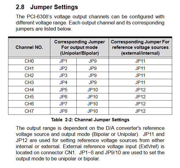
Complete configuration through board jumpers JP1-JP8, JP9/JP10, JP11/JP12:
JP1-JP8: Set the corresponding channel unipolar/bipolar output mode;
JP9/JP10: Grouping channel mode control;
JP11/JP12: Select DAC reference source: internal REF102 or external ExtVref (DB37 pin 6).
Default factory configuration: ± 10V bipolar, internal reference voltage.
3. Definition of CN1 DB-37 pins
Key signal grouping:
Voltage output V0-V7; PCI-6308A current output A0-A7;
Simulated ground AGND; ± 15V auxiliary power supply; ExtVref external reference input;
DI0-DI3 (digital input), DIGND (DI isolated ground);
DO0-DO3 (open drain digital output), DOGND (DO isolated ground).
4. Hardware installation steps
Turn off the power of the entire PC; Release static electricity from the human body;
Set board jumper; Insert any 32-bit PCI slot; Screw fixed baffle;
Power on, PCI Plug and Play PnP automatically assigns IO base addresses and interrupts by BIOS, and resources cannot be manually modified;
Windows system recognizes new hardware and installs PCIS-DASK driver.
Register mapping (underlying IO access)
The board uses PLX PCI-9052 bridge chip; PCI BIOS allocates IO base address.
DA output register (write only, 16 bit): Base+00h~Base+0Eh, 8 channels, 12 bit data; After writing the register, the hardware updates the output in approximately 13.96 μ s; The Data_Send status bit can be read to determine whether the DA conversion is complete.
DO register (Base+40h, write only): bit0-bit3 controls DO0-DO3; High position is invalid.
DI register (Base+40h, read-only): read DI input from bit4 to bit7; Bit0-bit3 reads back the DO output status.
DA digital format: 12 bit numerical value 0-4095 (0x000-0xFF), corresponding to analog output based on jumper single/bipolar mapping.
Example: ± 10V mode, 0 → -10V, 2048 → 0V, 4095 →+9.99969V.
Working principle
Voltage output: AD7564 multiplication DAC; Internal REF102 10V reference, or external pin input reference; Jumper switch between single/double polarity. Write a 12 bit digital code and wait for hardware setup time. The software needs to query the Data_Send status bit to avoid writing again before completion.
PCI-6308A current output: Each Vout is fed into the XTR110 chip, converting voltage to current; Software: 6308_S2V_Control: Set all 8-channel current ranges globally.
Isolation DI: Optocoupler isolation, with bidirectional TVS protection, 2.4k Ω current limiting resistor, supporting external sensor input up to 34V.
Isolation DO: The optocoupler drives the open drain transistor and requires an external pull-up resistor. The maximum external power supply is 24V.
Software Drivers and Programming Libraries
1. Support platforms and third-party software
DOS、Windows95/98/NT/2000/XP; Linux(PCIS‑DASK/X)。
Driver kit PCIS-DASK (Windows); PCIS‑DASK/X(Linux)。
Third party tool drivers (some require license): LabVIEW (DAQ-LVIEW free) HP‑VEE、DASYLab、ActiveX (PCIS‑OCX); InTouch (DDE), ISaGRAF soft PLC, InControl, OPC Server.
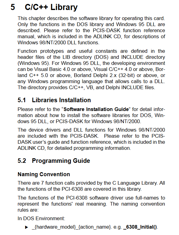
2. Core API of C/C++Library (DOS/Win95 DLL)
Add W_ to the prefix of Windows 95 DLL function names.
|Function | Function|
|_6308_initial() | Card initialization must be called first to obtain the number of cards and PCI information|
|_6308_Software_Seset() | Software resets IO register without restarting PCI hardware|
|_6308_da() | Single channel DA output write value (ch0-7, 12 bit data)|
|_6308_CA_0_3() | Simultaneously update channel 0-3 four DA channels|
|_6308_CA_4_7() | Simultaneously update four DAs of channels 4-7|
|_6308_Set_Status() | Read the busy status of DA sending and determine if the conversion is complete|
|_6308-DI() | Read the status of 4 isolated DI inputs|
|_6308_SO() | Set 4 isolated DO outputs (0-15)|
|_6308_S2V_Control() | Only PCI-6308A, set V-I current range mode|
Data type: U8/I16/U16/I32/U32/F32/F64 Boolean type, header file Pci_6308. h.