ADLINK PXIe-9848 8-channel 14 bit, up to 100MS/s synchronous sampling PXIe high-speed digitizer
Product Overview and Core Features
Analog acquisition: 8-channel single ended synchronous 14 bit ADC; The maximum sampling rate is 100MS/s, and the frequency can be divided as low as about 1.025kS/s; The simulation bandwidth software can be selected as 100MHz/20MHz.
Input front-end: software AC/DC coupling; Impedance can be switched between 50 Ω/1M Ω; AC coupling high pass angle is about 10Hz; range is only in two levels: ± 0.2V, ± 2V; maximum input overvoltage is ± 5V.
Onboard storage: 512MB onboard memory, independent FIFO depth of 32M sampling points per channel.
Bus DMA: PXIE Gen1 x4; Support Scatter Gather DMA, handle system non contiguous memory, and achieve high-speed streaming disk; Do not enable the maximum single transmission of 8MB for clustering.
Clock system: internal 10MHz crystal oscillator; Support PXIe backplane PXI_CLK10 and PXIe_CLK100 as reference clocks for multi module synchronization.
Automatic calibration: Built in+2.5V onboard reference source, no need for external instruments to complete self calibration; EEPROM stores multiple sets of calibration coefficients.
Front panel interface (all SMB threaded interfaces)
CH0-CH7: 8 analog inputs;
TRG IN: External digital trigger input.
Typical Applications
Radar signal acquisition, intermediate frequency spectrum monitoring, fiber optic testing, power supply unit PSU testing, cable fault location, and power partial discharge monitoring.
Key electrical specifications
Analog input
Item Parameter
Channel 8 single ended synchronization, 14 bit ADC
The maximum sampling rate is 100MS/s, and the minimum is about 1.025kS/s
Simulated bandwidth (-3dB) software optional 20MHz/100MHz
Input range ± 0.2V, ± 2V
Input impedance software switch between 50 Ω/1M Ω
Coupling AC/DC, AC coupling -3dB ≈ 10Hz
Overvoltage tolerance ± 5V
Misalignment error ± 1mV
Gain error ± 0.5%
Data format 16 bit 2 complement, valid 14 bits, low 2 bits need to be discarded by software
Time based clock
The accuracy of the internal oscillator is less than ± 25 ppm;
Multiple card clock synchronization can be achieved by using the backplane PXI_CLK10 and PXIe_CLK100 as reference clocks;
The actual sampling rate is obtained by dividing the 100MHz main clock using a 16 bit ScanIntrv scanning interval counter.
Trigger the system
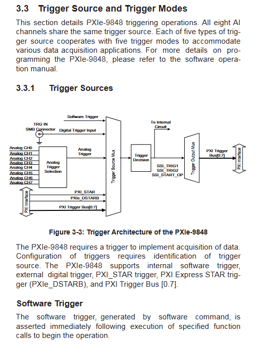
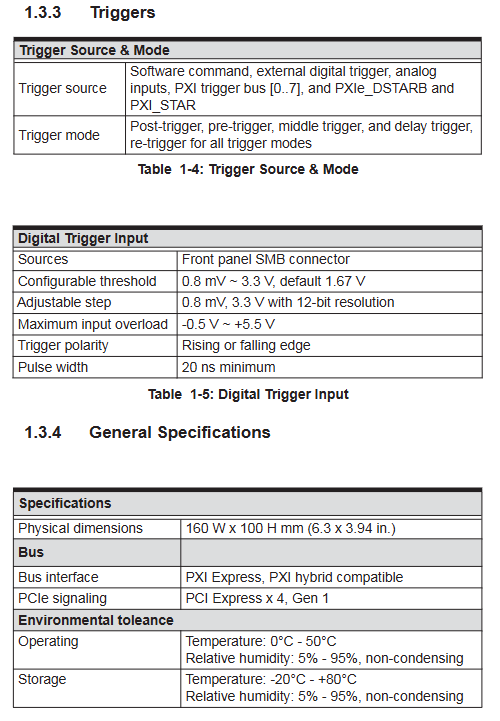
All 8 channels share the same trigger source. Trigger source: software trigger, external digital trigger (TRG IN SMB), 8-channel arbitrary analog trigger, PXI Trigger Bus [0-7], PXI_STAR, PXIe-DSTARB differential star trigger.
External digital trigger: threshold software programmable, 0.8mV~3.3V, 12 bit resolution, default 1.67V; rising/falling edge selection; Minimum pulse width of 20 ns, maximum input frequency of 25MHz; Input withstand voltage -0.5~+5.5V.
Simulation trigger: Choose one of the 8 channels as the trigger source; Trigger level with 14 bit resolution, supporting positive slope and negative slope triggering.
Trigger export: The module can act as a master to output triggers to any PXI Trigger Bus and synchronize with other slave modules.
Five triggering working modes
Post Trigger: After triggering, collect the set point count;
Pre Trigger: Save the sampling data before the triggering event;
Middle Trigger: Independently set the number of sampling points before and after triggering;
Delayed Trigger: After receiving the trigger, wait for a programmable delay before starting the acquisition;
Re Trigger: Supports multiple triggers, with each trigger collecting a set of waveforms that are automatically processed by hardware.
Hardware counter parameters
Explanation of the Range of Counter Bit Width Values
ScanIntrv 16 bit 1-65535 clock division, sampling rate=100MS/s ÷ ScanIntrv
DataCnt 32-bit 1-536870911 Total number of samples collected in a single session
TrigDelayTicks 16 bit 1-65535 delay triggered clock cycle count
ReTrgCnt 32-bit 1-536870911 acceptable trigger count for re triggering
Mechanical and environmental factors, power consumption
PCB size: 160mm × 100mm; PXI hybrid compatible module;
Working temperature: 0~55 ℃; Storage -20~80 ℃; Humidity 5-95% without condensation;
Power consumption:+3.3V standby 5350mA, full load 5900mA;+12V standby 470mA, full load 500mA.
Software driver system
Business drivers require authorization codes; Without authorization, only a 2-hour demo version can be run.
WD-DASK: underlying device drivers and DLLs, compatible with Windows 2000/XP/Vista/7; Can be called by VC++, VB, Delphi, etc.
DAQPilot SDK: A high-level development kit that supports VC.net, VB.net, BCB, and Delphi; Includes LabVIEW toolkit and MATLAB toolbox adaptation.
Note: This manual has an earlier version and uses WD-DASK instead of the later MAPS software stack, which is different from the PXIe-9834 and PXIe-9529H software systems.
DMA Data Transfer Instructions
When 8 channels are running at full speed of 100MS/s, the theoretical data throughput can reach 1.6GB/s, exceeding the theoretical bandwidth of PXIe Gen1 x4 (about 1GB/s).
Full speed 8 channels cannot be continuously streamed without restrictions; To achieve infinite streaming, the sampling rate must be reduced or the number of enabled channels must be minimized.
On board FIFO for data buffering; Scattered clustered DMA links fragmented system memory into linked lists; The maximum single transmission in non aggregated mode is 8MB.
Hardware installation
Static sensitive devices are strictly prohibited from hot plugging; Disassembly and assembly must be completely powered off, and anti-static wristbands and pads must be worn.
Turn off the power supply of the PXI chassis and keep the power cord grounded;
Align the module with the slot rail of the chassis and push it in. Tighten the red pop-up handle and hear a clicking sound. Tighten the panel screws;
Power on and install the WD-DASK driver recognition hardware in the system.
Packing list: PXIe-9848 module, All in One CD, user manual.
Multi module synchronization mechanism
8 channels within a single module share the same clock and trigger, naturally synchronized.
Clock synchronization: All modules use the backplane PXI_CLK10 or PXIe_CLK100 as a reference.
Trigger synchronization: The main module outputs a trigger signal to the PXI Trigger Bus; Select the corresponding PXI Trigger Bus from the module trigger source; It is also possible to use PXI_STAR/PXIe-DSTARB differential star triggering.
Calibration Mechanism
The onboard EEPROM is divided into three storage banks:
Bank0 (factory area, write protected): Factory calibration constant, will not be overwritten by self calibration.
Bank1 (User Area): Save the user’s Auto Calibration automatic calibration results.
The software can be configured to load Bank0 or Bank1 by default upon startup, and to permanently save the EEPROM.
Auto Calibration Automatic Calibration
Using onboard+2.5V internal reference source, no external signal source required, compensating for gain and offset temperature drift;
Suggestion: Preheat for at least 20 minutes when powered on, disconnect the external input cable before performing calibration;
Drive internal automatic compensation calibration delay, user program does not require manual processing.
Safety instructions and technical support
Static electricity protection; Power off disassembly and assembly; Stay away from liquids; Ventilation and heat dissipation; Incorrect lithium battery model poses a risk of explosion; Authorized engineers only for repairs.
Compliant with RoHS and WEEE environmental regulations.
Provide contact information for global branches in China (Shanghai, Beijing, Shenzhen), the United States, Europe, Japan, South Korea, Singapore, India, Israel, and other countries.
Comparison of Key Differences between PXIe-9848 and PXIe-9834
Project PXIe-9848 PXIe-9834
Channel 8CH, 14 bit 4CH, 16 bit
Maximum sampling rate 100MS/s 80MS/s
Bandwidth 20/100MHz, software optional fixed 40MHz
Range: ± 0.2V, ± 2V ± 0.5V/± 1V/± 5V/± 10V
512MB onboard memory, 32M independent per channel, 1GB shared memory
Impedance 50 Ω/1M Ω 50 Ω/1M Ω
Software Stack WD-DASK/DAQPilot (Old Version) MAPS (New Version Software Stack)
Trigger threshold external digital trigger software adjustable 0.8mV to 3.3V external digital trigger fixed TTL level
EEPROM calibration Bank 3 groups 2 groups (Bank0/Bank1)
If you need, I can compile a brief parameter lookup table for PXIe-9848.