ADLINK Express-BASE7 User Manual
Product positioning and applicable scenarios
1. * * Core Purpose * *: Standard ATX industrial carrier board, compatible with COM Express Type7 Basic/Compact modules, providing complete peripheral expansion, debugging, and remote management capabilities, replacing fully customized baseboards for early software and hardware verification.
2. * * Supporting components * *: OMe Type7 module, Express-BASE7 carrier board, supporting 10GbE daughter card (SFP+optical port/10GBASE-T electrical port optional), SATA storage.
3. Development advantages: Compared to designing the base plate from scratch, the development cycle is shortened by half. It comes with rich standard interfaces and debugging hardware, and is suitable for prototype development of data acquisition, network computing, industrial control, and remote operation and maintenance equipment.
Core Features and Functions
1. PCIe and 10 Gigabit Ethernet Expansion
-A total of 32 PCIe channels are led out by COMe modules;
-Exclusive x16 slot (PCIEKR) for 10GbE daughter cards, supporting 4 10GBASE-KR signals, with two optional daughter cards:
-SFP+daughter card: 4-channel fiber 10G;
-10GBASE-T daughter card: 4-channel copper cable 10G;
-Additional standard PCIe slots: 1 × x16, 2 × x8, for acquisition cards GPU、 Expansion of peripherals such as acceleration cards.
2. IPMI MiniBMC Remote Management
Equipped with MiniBMC controller, connected to onboard gigabit network through NC-SI, supporting:
Remote power on/off/reset, voltage (12V/5V/3.3V) monitoring, serial port redirection SOL; Local KCS channel management; Functions are selected according to the project.
3. Onboard Super I/O
Winbond W83627DHG-PT (wide temperature -40~85 ℃) LPC bus Super I/O, providing 2 DB9 serial ports, PS/2 keyboard and mouse, hardware monitoring, to compensate for the shortcomings of COMe module without traditional IO, and can be enabled/disabled by jumper switch.
4. Dual SPI BIOS Switching (Secondary BIOS)
On board U55 SPI BIOS chip, choose between using the built-in BIOS of COMe module or the secondary SPI BIOS on the board through JP23/JP24 jumper; Used for firmware debugging, new version testing, and module BIOS damage recovery.
5. Complete set of debugging hardware
-Two digit+four digit POST digital display;
-Single step BIOS execution mode (jumper switch+onboard manual switch), firmware troubleshooting;
-LPC debugging pin, convenient for logic analyzer to capture bus signals.
6. Status indication and hardware buttons
-LED indicator lights: power, standby, hard drive activity, watchdog, module type recognition;
-Physical micro switches S1~S4: ATX power supply, reset, Lid cover detection, sleep ACPI switch; There is also a S5 MiniBMC reset button (dedicated for firmware debugging).
7. Enrich industrial peripheral bus
Dual SATA, 4-channel USB 3.0, Gigabit RJ45, multi-channel serial port I2C/SMBus、 8-channel GPIO, 3-channel temperature controlled fan, watchdog, hardware temperature and voltage monitoring.
Hardware architecture and mechanical specifications
1. Board Layout and Signal Block Diagram (Chapters 3 and 4)
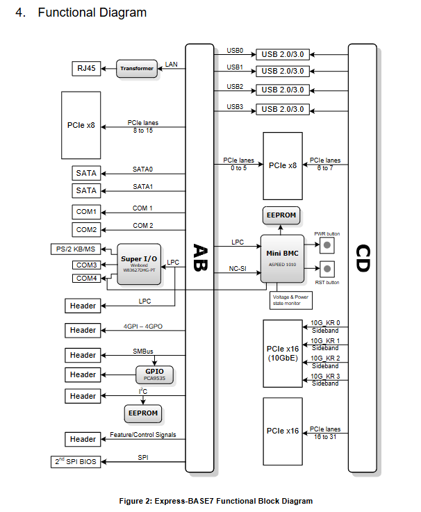
-Onboard core components: MiniBMC, W83627 Super I/O, secondary SPI BIOS, PCA9535 GPIO expansion, four-way SATA, multi-channel USB, PCIe expansion slot, 10G dedicated slot;
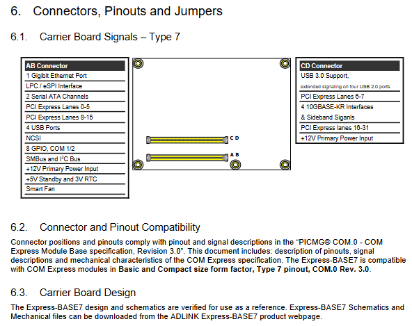
-COMe AB/CD dual row 110 pin connector: complete output of gigabit network, 4 x USB 3.0, 32 PCIe, 4 channels of 10G-KR, SATA, LPC/eSPI, I2C/SMB, GPIO, serial port, power supply, NC-SI remote management signal. The manual includes a complete A/B/C/D signal definition table for each pin.
2. Mechanical dimensions
Standard ATX specifications, drawing units in millimeters, general tolerance ± 0.25mm, module positioning hole accuracy ± 0.10mm, including all installation holes and connector position dimension drawings.
Detailed definitions of all connectors, jumpers, and switches (Chapter 6, core chapter of the manual)
1. COMe AB/CD Mother Seat
Complete 110 pin A/B/C/D quad pin table, defining Gigabit Ethernet, USB 3.0, PCIe 0-31 channels, quad 10G-KR, SATA, LPC, SMBus, I2C, GPIO, serial port NC-SI、 All signals including 12V/5V RTC power supply, watchdog, temperature alarm, low battery voltage, etc.
2. 10GbE proprietary PCIEKR x16 slot
Independent pin definition, including four 10G transceivers, SFP I2C, PHY reset, interrupt, and various power supplies, can only be used with two original 10G daughter cards and cannot be used with standard PCIe devices.
3. Standard PCIe slot (1×16/2xx8)
Define PCIe differential transceiver, reference clock, reset, SMBus, JTAG debugging, standby power, wake-up signal for standard peripherals such as DAQ and accelerator cards.
4. Network interface, storage USB、 Serial port peripheral connector
1. Gigabit RJ45 (CN18): 8-pin Gigabit differential signal;
2. SATA (CN12/CN13): Standard 7-pin SATA signal;
3. CN45 four-way USB 3.0 female socket: USB2 compatible+USB3 high-speed differential;
4. Serial port:
-CN1002: Super IO leads to COM3/4 DB9;
-CN6/7: COMe module native SER0/SER1 pin serial port;
-CN22 IrDA infrared pin;
5. PS/2 key mouse split pin;
6. User bus 4-pin connectors for I2C (CN33) and SMBus (CN34);
7. Multiple GPIO pins CN36/CN41/CN42, with 16 channels of digital IO extended through PCA9535 and matched with status LED;
8. Three 4-pin temperature controlled fan sockets (FAN1/FAN2/FAN3), supporting speed detection and PWM speed regulation;
5. Power connector and power jumper logic
1. CN1:24pin standard ATX main power supply;
2. CN5: 4pin ATX 12V independent power supply, * * must be plugged in to power the COMe module * *;
3. Complete power configuration jumpers (JP1/JP2/JP3/JP34, etc.):
-JP1: AT/ATX mode switching;
-JP2: S3/S5 standby power selection;
-JP3: 5VSB standby power source;
-JP34: 12V output on/off in S3/S5 state;
The manual provides a jumper combination table for four power supply schemes (ATX power supply/AT power supply combined with AT/AT mode module).
4. CN44 intelligent battery plug;
6. Function configuration jumper
1. JP4: Clear CMOS Clear CMOS jumper;
2. JP18: Super I/O enabled/disabled;
3. JP10/JP11: Super I/O address (2E/4E), clock frequency (24/48MHz);
4. JP23/JP24: Switching between primary and secondary BIOS;
5. JP25/JP26: LPC EEPROM address;
6. JP19~22: I2C/SMB signal buffer bypass;
7. JP29~31: I2C EEPROM address configuration;
8. JP32: TPM signal pull-up;
9. CN46~49 MiniBMC mode jumper: normal/debug mode switching;
10. CN1003/004: Serial port routing, optional to directly output DB9 or connect to MiniBMC to achieve SOL serial port remote control;
7. Debugging specialized connector
CN37/CN40 LPC debugging pin, captures the LPC/eSPI bus, used for BIOS single step debugging and POST troubleshooting.
Multi functional miscellaneous pin CN32
Integrated power LED, WDT light, buzzer, reset, hard disk indicator light, power button, temperature alarm, GPIO and other system status signals.
Secondary SPI BIOS
1. Hardware: U55 8-pin SPI Flash socket, jumper JP23/JP24, choose one BIOS source;
2. Purpose:
-Testing has not released a new version of BIOS firmware;
-Customize and modify firmware development;
-System recovery after COMe onboard BIOS damage;
3. Switching operation: Turn off the power and adjust the jumper, replace the SPI chip to switch the startup firmware.
Switches, LEDs, and Debugging Display
1. Physical switch S1 power supply, S2 reset, S3 sleep, S4 cover detection, S5 MiniBMC debugging reset;
2. LED array:
-5VSB standby, main power, hard disk read/write, S3 sleep status indicator light;
-The COMe Type model with 7-channel LED recognition insertion;
-Digital IO corresponds to LED, lit at high level;
3. POST debugging: Two digit basic POST code+four digit address digital tube, supporting single step BIOS execution debugging mode.
Safety Notice
-Only match the rated voltage on the nameplate for power supply, avoiding liquids, moisture, and heat sources;
-Reserve ventilation in the chassis and prohibit blocking the heat dissipation openings;
-Disconnect all power cords before disassembling the machine;
-RTC lithium battery warning: There is a risk of explosion if the model is incorrect. Scrap and recycle according to regulations;
-If there is cable damage, water ingress, or falling damage, please contact the official repair team and do not attempt to open the cover for repairs.