ADLINK NuPRO-850 Full length ePCI-X Industrial Control Board
Chapter 1 Product Introduction (Specifications, Architecture, Standard Accessories)
Factory packing list
NuPRO-850 motherboard, paper manual, driver CD, serial port cable, dual USB ribbon cable, CPU cooling kit, 2 ATA100 IDE cables, 2 SATA data cables; OEM customized versions may have differences in accessories; Throughout the operation, anti-static measures must be taken and an anti-static wristband must be worn.
Core hardware features
Bus standards: PICMG1.2 embedded PCI-X, PCI2.2 specifications, dual independent buses: BusA 64bit/66MHz PCI-X, BusB 32bit/33MHz PCI; Single MiniPCI III expansion slot.
Processor: FC-MPGA478 Pentium 4, 0.13/90nm process, supports hyper threading; FSB 400/533/800MHz, The highest frequency is 3.4GHz, and the second level cache is 512KB/1MB.
Memory subsystem
4-channel 184 pin DDR DIMM slot, dual channel architecture, supports 266/333/400MHz ECC/non ECC buffer free memory, maximum 1GB per unit, maximum 4GB for the whole machine; dual channel requires paired installation of memory of the same specification, does not support register type memory.
Graphic Display
ATI Mobility M9 (AGP4X)/M10 (AGP8X) dedicated graphics, with 64MB of onboard memory; Supports three independent outputs: rear VGA, onboard second CRT pin, and 24 bit LVDS LCD screen; Hardware jumpers can shield onboard graphics cards.
Internet
Intel 82547GI Gigabit Ethernet card, connected to 875P CSA high-speed channel, supports 10/100/1000M adaptive, IEEE802.3x traffic control, and PXE diskless network boot. RJ45 comes with dual color link/rate indicator lights.
Storage interface
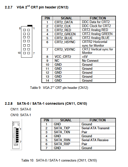
Dual Ultra DMA10 IDE channels (up to 4 IDE devices), 2 SATA 150MB/s interfaces.
I/O peripherals
Rear mounted 2 USB 2.0 ports, onboard expansion 2 USB ports (total 4 ports); 1 RS232 16550 serial port; AC’97 2.2 audio (requires optional DB-AC97 daughter card).
Industrial control specific functions
W83L784R hardware monitoring chip: collects CPU/motherboard temperature, dual fan speed, and various DC voltages of the entire board;
Two level programmable watchdog WDT: timing 1-255 seconds/1-255 minutes, timeout can trigger interrupt+machine reset;
Chassis open cover intrusion detection, 8MB erasable Award/Phoenix BIOS (software lock protected Flash).
Hardware architecture diagram
The CPU is connected to an 875P MCH northbridge via FSB, which controls dual channel DDR, AGP graphics cards, and gigabit CSA networks; The North Bridge DMI link connects to the 6300ESB South Bridge, which branches off the PCI-X/PCI bus MiniPCI、IDE/SATA、USB、AC97、 Super IO, watchdog, hardware monitoring module.
Mechanical and environmental parameters
Size: Full length industrial board 338.6mm × 122mm;
Working temperature of 5-55 ℃, storage temperature of -40~70 ℃, humidity of 5%~95%, no condensation;
Certified CE/FCC Class A, with UL-94V flame retardant rating for onboard plastic.
Chapter 2: Complete Definition of Connectors and Jumpers
2.1 Overview of Board Layout
Distinguish between front and rear panel interfaces, onboard pins, jumpers, memory slots, CPU sockets, and dual ePCI-X gold finger buses, and label all CN interface numbers and JP jumper numbers.
2.2 Rear I/O interface pins
VGA、 Dual USB, Gigabit RJ45, COM1 serial port, complete pin signal definition, network port dual color light status description.
2.3 Onboard built-in pins (full pin comparison table)
Coverage: AC97 audio, chassis open cover detection CN1, front panel pins (power/reset/hard disk light/watchdog indicator light/beep), second CRT display pin, LVDS LCD screen, dual SATA, primary/secondary IDE, CPU fan/graphics card fan power supply, MiniPCI slot, ATX 12V auxiliary power supply.
2.4 Function jumper
JP1 Clear CMOS: Power off and short circuit to clear BIOS parameters, repair startup faults;
JPY1 VGA shielding jumper: Short circuit to disable onboard ATI graphics card, used when connecting an external independent AGP card.
Chapter 3 Hardware Installation Operation Guide
3.1 CPU installation steps
Lift the Socket478 pressure rod, align the CPU triangle with the slot positioning angle, and lay it flat;
Press down the buckle to lock it in place; Apply thermal conductive silicone grease evenly and match it with the original heat dissipation kit;
The fan cable is connected to the FN2 CPU fan socket, and if there is no heat dissipation, it will overheat and crash.
3.2 DDR Memory Installation
The slot has a foolproof notch, and dual channels must be paired with DIMM1+DIMM2/DIMM3+DIMM4 for optimal memory performance with the same capacity and frequency; Single channel can be used individually.
3.3 IDE hard drive wiring
The 40 pin ribbon cable distinguishes between master/slave disks, with the main IDE CN7 and secondary IDE CN4. The red line of the ribbon cable aligns with pin 1 of the interface.
3.4 Basic BIOS Operations
Press Del to enter the Award/Phoenix Plug and Play BIOS during startup, where you can modify the startup sequence, hardware parameters, and power management; The configuration is stored in RTC battery CMOS and supports two-level boot passwords.
3.5 Key points of operating system installation
Adjust the first boot device (CD/floppy drive/USB) in BIOS; After the system installation is completed, install the complete set of original drivers in order, compatible with Windows 2000/XP, Red Hat Linux 7.3 and above.
Chapter 4 Driver Installation Specification (Windows Platform)
The driver CD is divided into four major directories: chipset, graphics card, network card, and watchdog. It must be installed in order and restarted at each step
Intel 875P/6300ESB chipset INF driver: underlying bus, SATA/USB/PCI resource recognition foundation;
ATI M9/M10 graphics card driver: supports dual CRT+LVDS multi display output;
Intel 82547GI Gigabit Network Card Driver: Comes with network diagnostics and load balancing tools;
The watchdog matching test program HRWDT.EXE can directly debug the timer function.
Chapter 5 Development Core of Watchdog Timer (WDT)
6.1 Hardware Architecture
Integrated into the 6300ESB South Bridge, a 35 bit subtraction counter with two-stage segmented timing: the first stage generates an internal interrupt upon timeout, and the second stage outputs a WDT_TOUT # hardware reset signal upon timeout, supporting a wide timing range of 1 μ s to 10 minutes.
6.2 Register operation logic
Core registers: preload register 1/2, interrupt status register, reload register, configuration latch register;
Unlocking rule: The timing value can only be modified after writing the sequence of 0x80 and 0x86;
Two working modes
Standard WDT mode: two-level timing, software periodically reloads to feed dogs;
Free running mode: Single segment automatic loop, no need to continuously feed the dog.
6.3 Supporting Resources
Provide DOS debugging tool HRWDT.EXE, which provides a complete operation process for register read and write, dog feeding, and timer shutdown. It can be embedded in unmanned industrial control programs to prevent crashes.
Chapter 6 ePCI-X Bus Technical Specification
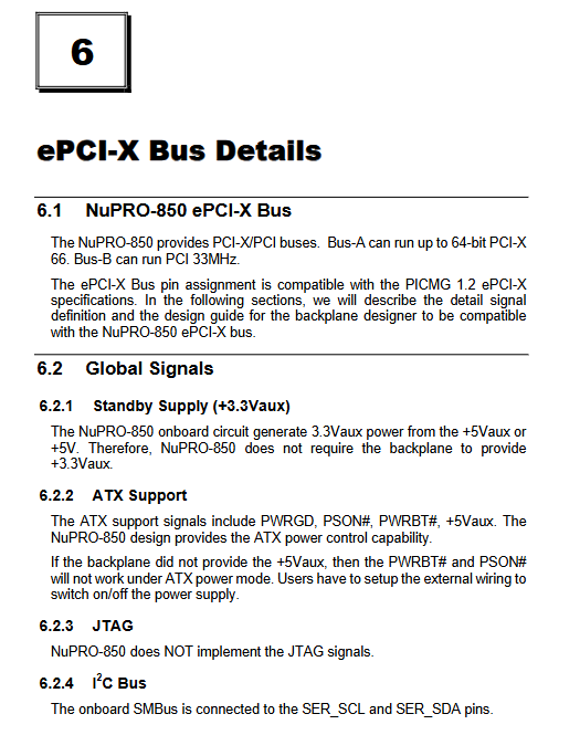
Dual bus separation design: BusA 64bit PCI-X 66MHz (high-speed acquisition/motion card), BusB 32-bit PCI33MHz (general-purpose peripheral);
Backplane compatibility signals: ATX power control, 3.3V auxiliary standby, SMB system management bus, PME remote wake-up, backplane in place detection;
Limitation: The board does not output JTAG debugging signals, and the backplane VIO voltage detection is used for hardware error prevention.