ADLINK DAQ/DAQE/PXI-220x series multifunctional acquisition card
Product Overview and Hardware Specifications
1.1 Core differentiation of four models (core differences in AI performance)
Model, Channel Scale, ADC Bit Number, Highest Sampling Rate, Featured Configuration
2204 64 single ended/32 differential 12 bit 3MS/s single channel, 1MS/s multi-channel with 4 synchronous digital input SDI, 2 AO, 2 GPTC
2205 64 single ended/32 differential 16 bit 500kS/s high-precision, 2-channel AO, 2-channel GPTC
2206 64 single ended/32 differential 16 bit 250kS/s low noise, 2-channel AO, 2-channel GPTC
2208 96 single ended/48 differential 12 bit 3MS/s single channel, 1MS/s multi-channel without AO or GPTC, with the highest number of channels
1.2 Core Hardware Function Modules
(1) Simulate input AI
Flexible channel configuration: software switches between single ended RSE/NRSE, differential DIFF, and supports mixed acquisition; Customizable 512/1024 length channel gain queue, freely defining acquisition order, range, and gain.
Programmable gain:
2204/2208:×1/×2/×4/×5/×8/×10/×20/×40/×50/×200
2205/2206:×1/×2/×4/×8
Input range: Bipolar ± 10/± 5/± 2.5/± 1.25V; Unipolar 0~10/0~5/0~2.5/0~1.25V; Supports ± 30V overvoltage protection and ± 15V power-off protection.
Electrical specifications: Input impedance 1G Ω, DC-60Hz maximum 93dB common mode rejection CMRR; Built in 40MHz time base, supporting 1-40MHz external clock; 1024 word onboard AI FIFO cache.
Synchronous sampling output SSHOUT: It can be connected to an external sample and hold chip to achieve multi-channel synchronous acquisition (2208 does not have this function).
(2) Analog output AO (not supported by 2208)
2-channel 12 bit DAC, with a maximum update rate of 1MS/s; Single channel 1024 word FIFO, dual channel 512 word FIFO each;
Support internal 10V reference/external AOEXTREF reference, output ranges of ± 10V/0~10V, etc; Short circuit protection, maximum output current ± 5mA.
(3) Digital IO DIO
24 channel universal TTL bidirectional IO (82C55 chip, PA/PB/PC three ports), default high impedance input when powered on; 2204 is equipped with an additional 4 SDI synchronous digital inputs, which are synchronized with AI sampling and locked into the same 16 bit data word.
(4) Universal Timer GPTC (not supported by 2208)
Two independent 16 bit up and down counters, supporting internal and external 10MHz clocks, software and hardware gating, and direction control; Built in 8 working modes: event counting, cycle measurement, pulse width measurement, single/continuous pulse generation, re triggered pulse, etc.
(5) Synchronous Interface SSI
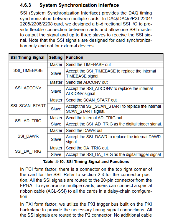
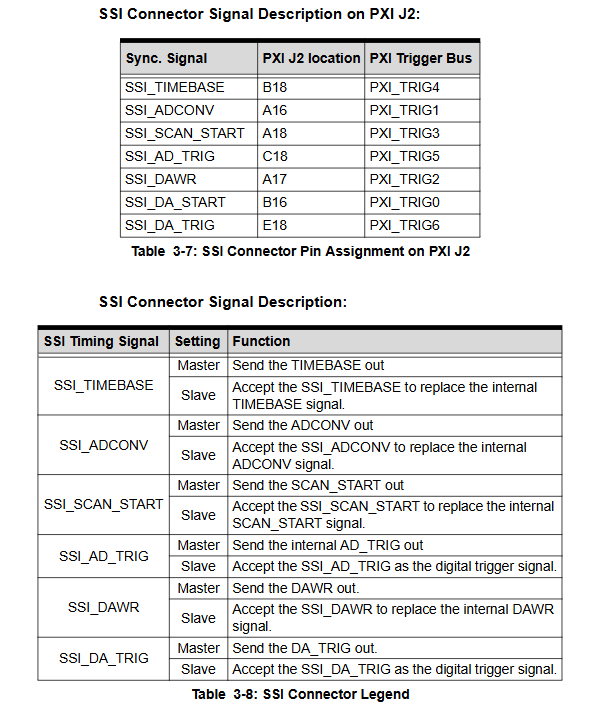
20 pin synchronous bus, 7 synchronous timing signals, realizing clock, trigger, and scan synchronization of multiple DAQ cards; PXI version can reuse chassis J2 trigger bus.
1.3 Trigger System (AI/AO share a set of trigger sources)
4 categories of trigger sources, 4 acquisition timing modes:
Trigger source: software trigger, external digital trigger EXTDTRIG, external analog trigger EXTATRIG, SSI synchronous trigger;
Simulate triggering with 5 criteria: above threshold, below threshold, within interval, high hysteresis, low hysteresis, supporting programmable hysteresis voltage;
Four collection modes: pre trigger (storing data before triggering), intermediate trigger (storing data before and after triggering), post trigger (only after triggering), and delayed trigger (collecting data after triggering); All support can be triggered again, with limited/infinite loop collection.
1.4 Data transmission method
Software polling: low-speed single point acquisition, with CPU fully involved throughout the process;
Bus Master DMA (Scattered/Gather): High speed data acquisition, hardware direct write memory, support for large continuous data, no memory fragment limit, is the only transmission method that supports pre/intermediate triggering.
1.5 Physical and Electrical Parameters
Interface: Dual 68 pin VHDCI (CN1 analog, CN2 hybrid IO)+20 pin SSI synchronous interface;
Power supply: DACe (PCIe) with multiple 3.3V power supplies, DAQ/PXI with only 5V; power consumption of 0.95A~1.3A (+5V);
Environment: Working temperature range of 0-55 ℃, storage temperature range of -20~80 ℃, humidity range of 10%~90%, no condensation.
1.6 Supporting software MAPS full ecosystem
MAPS Core (essential underlying layer)
ACE (ADLINK Connection Manager): Device recognition, DMA cache allocation, device aliases; Built in Soft Front Panel for visualizing waveform acquisition and manually controlling AI/AO/DIO/GPTC; Provide chassis monitoring and hardware self-test tools.
MAPS/C:Windows C/C++ SDK, Head file API、 Complete engineering example;
MAPS/LV: LabVIEW dedicated VI library, compatible with various testing programs;
MAPS/C #:. NET C # Development Kit (documentation to be released);
Authorization mechanism: Unauthorized trial only lasts for 2 hours, formal authorization requires purchasing from distributors.
Hardware Installation, Jumping and Configuration
2.1 Packaging and anti-static specifications
The packaging includes a collection card, paper manual, and software installation guide; The board is an electrostatic sensitive device, and must be operated with a grounded anti-static wristband and anti-static pad. Only hold the edge of the board and strictly prohibit touching the chip’s gold fingers; Before powering on, check if the socket IC is compacted and do not turn on if it is damaged.
2.2 Board Layout Differentiation
DACe (PCIe): sub motherboard architecture, board to board connectors transmit signals;
DAQ (Standard PCI): CN1/CN2 dual 68 pin front panel, side SSI socket, standard PCI gold finger;
PXI (3U cPCI): Compact chassis version, front locking buckle, chassis side PXI triggers J2 multiplexed SSI signal.
2.3 Jumper/dip switch (without IRQ/base jumper, fully software plug and play)
SW1 4-digit DIP dialing: Board ID numbers 0-15, distinguishing device numbers for multi card systems; The driver tool defaults to ignoring IDs and needs to manually uncheck and enable them;
JP4 jumper: Enable DIO power on pull-down (default short circuit, IO initial low level), disconnect to power on IO high resistance.
2.4 PCI/PnP Plug and Play
The system BIOS automatically allocates IRQ, IO base address, and DMA resources without the need for hardware jumpers; The faults are mostly interrupt conflicts, and it is necessary to enter BIOS to adjust PCI resource allocation.
Connector Pin and Analog Signal Wiring
3.1 Definition of connector pins
CN1: Main analog channel, AI positive and negative differential pins, EXTATRIG external analog trigger, AISENSE common mode reference, AIGND analog ground; 2204/06 has 64 channels, while 2208 has been expanded to 96 channels;
CN2: Mixed signal interface, AO output, digital IO PA/PB/PC, GPTC clock/gate/output, EXTDTRIG digital trigger, EXTTIMEBASE external time base, SDI synchronous input (only 2204);
SSI 20 pin: Multi card synchronous timing, including global time base, scan start, AD/DA trigger synchronization signal, PXI can be mapped to the chassis J2 trigger bus.
3.2 Three types of analog input wiring schemes
RSE single ended: signal connected to AI, reference board AIGND, compatible with floating signals such as thermocouples and isolation transmitters;
NRSE single ended: The signal is locally grounded to the AISENSE pin, eliminating multiple ground potential differences and adapting to mains power supply grounding equipment;
DIFF differential: AIH connected to positive signal, AIL connected to negative signal, with the strongest common mode noise suppression; Floating sources require adding bias resistors at the negative end to provide a return path, which is preferred for industrial anti-interference.
Basic Working Principles (Core Development Reference)
4.1 A/D acquisition principle
4.1.1 Two collection modes
Software single point conversion: single trigger single channel, timing controlled by software, suitable for low-speed single point measurement;
Programmable scanning acquisition (recommended for high speed): 4 sets of hardware counters for precise timing control:
SI2: Single channel sampling interval; SI: Complete scanning cycle; PSC: Total number of scans per trigger; NumChan: Number of channels in a single scan; Constraint SI ≥ SI2 × NumChan;
Data format:
12 bit (2204/2208): 12 bit AD+4 SDI synchronous digits (only 2204), 16 bit word storage;
16 bit (2205/2206): Pure 16 bit binary complement sampling data.
4.1.2 Detailed explanation of the four major triggering timing sequences
Pre trigger: continuous sampling, only retaining the first M scans after triggering; M-enable can block early triggers and ensure a fixed data length;
Intermediate triggering: Simultaneously store M scans before triggering and N scans after triggering, capturing the complete waveform before and after the event;
Post trigger: Collect N scans only after the trigger arrives, and support multiple re triggers;
Delay triggering: Wait for programmable delay after triggering, and start collection after the delay ends;
4.1.3 DMA Scattered Transmission
The hardware DMA controller directly reads and writes host memory, supports non contiguous memory block chain transfer, and has no upper limit for single acquisition; Circular linked lists can achieve continuous cyclic collection with extremely low CPU usage.
4.2 D/A waveform generation (2208 does not have this module)
Two output modes: software single point update and timed waveform generation;
5 sets of timing counters: UI (update interval), UC (single waveform point count), IC (waveform cycle count), DLY1 (trigger pre delay), DLY2 (waveform interval delay);
Three levels of stop mode: immediate stop, complete current waveform stop, complete entire loop stop; Supports finite/infinite waveform iteration and re triggered output.
4.3 Digital IO
24 channels of 82C55 programmable ports, PA/PB adjustable input/output, PC high and low 4-digit independent configuration; Power on all high impedance inputs; 2204 has a unique SDI synchronous digital input, which is synchronized with AI sampling and locked.
4.4 GPTC Timer 8 Working Modes
Covering gate event counting, signal cycle measurement, pulse width measurement, single/continuous trigger pulse output, supporting internal and external clocks, software/hardware gate control start and stop, and real-time readable count values without interruption.
4.5 Trigger Signal System
Simulation trigger: Any AI channel or independent EXTATRIG can be selected as the trigger source, with 8-bit programmable threshold, 5 criteria, and adjustable hysteresis;
Digital trigger: EXTDTRIG (AI trigger), EXTWFTRIG (AO trigger), supporting rising/falling edges, with a minimum pulse width of 10ns;
SSI synchronous triggering: Multiple cards share the clock, scan, and trigger signals to achieve synchronous acquisition of multiple devices.
4.6 Global timing synchronization with SSI
Built in multiple channels that can output timing signals (TIMEBASE, SCAN_START, ADCONV, DAWR, etc.), which can be connected to external circuits through AFI auxiliary pins and SSI bus; The SSI bus synchronizes multiple DAQs uniformly, eliminating the time difference of multi card sampling, and is suitable for multi-channel large-scale testing systems.
Calibration Function
Onboard 5V high-precision reference source (temperature drift ± 2ppm/℃, long-term stability 6ppm/kWh);
Auto cal automatic calibration: software one click calibration of AI/AO gain and offset errors;
Calibration constant read-write: can load factory calibration values, save custom calibration parameters, and not lose them when powered off.