ADLINK PCIe 7256 Industrial Digital I/O Board
Product Overview and Features
1.1 Core Features
Bus: PCI Express x1, plug and play;
16 channel lock relay output (Form-C/DPDT), can maintain output state when powered off; Onboard LED indicates relay status;
16 channel non-polar optocoupler isolated digital input; Jumper can choose AC filtering/unfiltered (DC) input mode; Support dry contact input; Isolation voltage 2500Vrms (channel to system);
Support COS (Change of State) interrupt, DI0 and DI1 can also be separately configured with rising edge interrupt;
Card ID dialing S1, distinguishing different cards when multiple cards are on the same host at the same time;
68 pin SCSI interface CN1 leads out all I/O; Support external LED (JP3/JP4);
Comes with isolation and 5V power supply, maximum output 170mA@40 ℃.
1.2 Typical Applications
Industrial switch control, external high-power relay drive, signal switching, laboratory automation, limit switch monitoring, contact status detection.
1.3 Key Electrical Specifications
Digital isolation input DI
Channel: 16 routes; Rated input current 10mA, maximum 50mA; supports up to 24V AC/DC;
Isolation: 2500Vrms channel system isolation; JP1 controls DI0-7, JP2 controls DI8-15, and the jumper selects AC filtering/DC (default DC without filtering).
Lock relay output DO
16 channel DPDT Form-C; Contact specifications: 125V AC/0.5A, 30V DC/1A;
The suction/release time is 3ms each; the contact resistance is 60m Ω; the insulation resistance is ≥ 1000M Ω @ 500VDC.
Physics and Environment
Size: 175mm × 107mm, PCIe half length card; Working temperature: 0-60 ℃; Storage -20~80 ℃; Humidity of 5-95% without condensation.
1.4 Software Support
PCIS-DASK: 32/64 bit kernel driver+SDK, supports Windows 7/8.1; Provide DLL, compatible with LabVIEW;
DOS environment provides C/C++function library; Drivers must be installed before installing the board.
Board hardware layout, connectors and jumpers
2.1 Components on PCB board
Identification name function
JP4 external LED connector
B JP3 external LED connector
C S1 Board ID 4-digit DIP dip switch
D JP2 DI8-15 AC/DC filter jumper
E JP1 DI0-7 AC/DC filter jumper
F CN1 68 pin SCSI I/O interface
2.2 CN1 68 pin SCSI connector
include:
Each relay circuit: NO (normally open), COM (common terminal), NC (normally closed);
DI0~DI15 isolated digital input; DICOM1 and DICOM2 are DI common terminals;
ISO5V isolated 5V output, ISOGND isolated ground.
2.3 Jumper JP1/JP2 Input Mode Settings
JP1 corresponds to DI0-DI7; JP2 corresponds to DI8-DI15;
Factory default: DC (non AC filtering, suitable for DC signals); Switch the jumper to the AC position to enable RC AC filtering and adapt to the AC input signal.
2.4 Board ID (S1 DIP dip code)
4-digit dip switch, 1=ON, 0=OFF; The ID value ranges from 0 to 15. In a multi card system, software relies on BoardID to distinguish between boards and avoid access conflicts.
2.5 External LED (JP3/JP4)
16 external LED channels can be connected for displaying relay status on the chassis panel;
The board is equipped with a 330 Ω current limiting resistor, and the forward voltage drop Vf of the LED must be less than 2V; pay attention to the polarity of the LED.
Hardware installation steps
Unpacking inspection: The accessories include PCIe 7256 board and quick start guide; Pay attention to anti-static measures, use anti-static bags and wristbands;
First install the driver software, then physically insert the card;
Turn off the host power, unplug the power cord, and open the chassis;
Align the gold finger of the board with the PCIe x1 slot and press it into place, then fix the baffle with screws;
Reinstall the computer case and power it on.
PCIe plug and play: Base address and IRQ interrupt number are automatically assigned by BIOS/system, without the need for jumper settings. If the system starts abnormally, investigate BIOS interrupt resource conflicts.
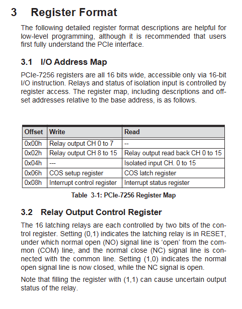
Register definition (low-level IO programming)
All registers are 16 bits wide and only allow 16 bit IO instructions to access, offset relative to the base address BASE:
Offset write function and read function
0x00 relay output CH0-CH7-
0x02 Relay Output CH8-CH15 Relay Readbacks CH0-CH15 Status
0x04- Isolation DI Input CH0- CH15
0x06 COS setting register COS latch register
0x08 Interrupt Control Register Interrupt Status Register
4.1 Relay output control register
Each channel of the latch relay occupies 2 bits:
DOx_S (set), DOx_R (reset);
(1,0) → SET, NO connects to COM;
(0,1) → RESET, NC connects to COM;
⚠️ Prohibit writing (1,1), relay status is unpredictable.
Read back register: bit=1 indicates relay SET; Bit=0 indicates RESET.
4.2 Isolated Digital Input Register (BASE+0x04 Read)
Bit x corresponds to DIx; 1=Input high level; 0=Input low level.
4.3 COS status change interrupt
COS setting register (0x06 write): bit set to 1, corresponding to DI channel open state change interrupt (both rising edge and falling edge triggered);
COS latch register (0x06 read): When a state transition occurs, the DI level is latched. After clearing the interrupt, the hardware automatically resets to zero, eliminating CPU polling.
4.4 Interrupt Control Register (BASE+0x08 Write)
Supports two sets of mutually exclusive interrupt modes, which cannot be turned on simultaneously:
Mode 1 COS Interrupt: An interrupt is triggered when the level of any DI channel that is turned on changes;
Mode 2 DI0/DI1 interrupt: only supports rising edge triggering, can choose DI0, DI1 single or dual path.
Register bit definition:
Bit0: COS_CLR (write 1 to clear COS interrupt)
Bit1: CHO_CLR (write 1 to clear DI0 interrupt)
Bit2: CH1_CLR (write 1 to clear DI1 interrupt)
Bit8: COS_int-IN enables COS interrupt
Bit9: CH0_Int-IN Enable DI0 rising edge interrupt
Bit10: CH1-INt-IN enables DI1 rising edge interrupt
4.5 Interrupt Status Register (BASE+0x08 Read)
Bit0=COS interrupt status; Bit1=DI0 interrupt state; Bit2=DI1 interrupt status; Simultaneously read back interrupt enable configuration bit.
It is illegal to open both COS Int-IN and CHO/CH1 Int-IN simultaneously.
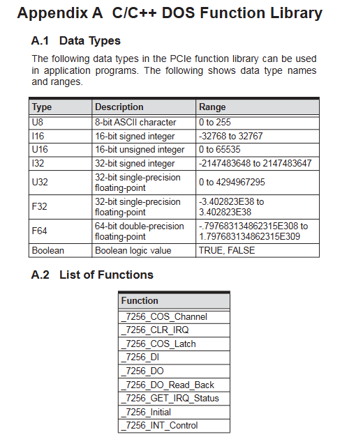
Appendix A C/C++Library Functions in DOS
Provide a set of DOS environment driver libraries, with main APIs:
_7256Initialize: Initialize by scanning the PCIe 7256 card of the system to obtain the base address and interrupt, which must be called first;
_7256-DO: Output, control latch relay SET/RESET;
_7256-DO-Read_Sack: Read the current status of the relay;
_7256-DI: Read all 16 DI inputs;
_7256_SOS_Channel: Configure which DI channels to enable COS state change detection;
_7256_SOS_Latch: Read the DI data obtained from the COS latch;
_7256-IND_Control: Set interrupt mode (COS/DI0/DI1);
_7256_ GET_SRQ_Status: Read interrupt status;
_7256_SLR_SRQ: Clear the interrupt request flag.
Data types: U8, I16, U16, I32, U32, F32, F64, Boolean.