ADLINK PCIe 7432 bus industrial isolated digital I/O board
Product Overview and Core Features
1.1 Main functional features
Bus: PCI Express x1, plug and play;
32 optocoupler isolation DI, 32 optocoupler isolation DO, channel system isolation voltage 2500Vrms;
DI channel is non-polar, supports source/drain wiring, with a maximum input of 24V AC/DC; Only DI0 and DI1 support interrupts;
DO stands for open collector of Darlington transistor (current output); Maximum single channel current 500mA@24V All channels simultaneously conduct the upper limit of the total current 120mA@24V The output voltage range is 5-35VDC;
Onboard isolation+5V power supply, maximum output 200mA@40 ℃;
The output is connected to inductive loads (relays, coils), and the external power supply VDD pin is matched with a flywheel diode circuit to suppress reverse high voltage and protect the output transistor.
1.2 Application Scenarios
Industrial and laboratory automation, watchdog WDT, event counting, frequency counting/pulse generation, low-level pulse generation, delay control.
1.3 Electrical specifications
Isolated digital input DI (32 channels)
Optocoupler model HCPL-814; Rated input current 10mA, maximum 20mA;
Input voltage: maximum 24V AC/DC; Logic low 0-1.5V; Logic high 5-24V; Input impedance 2.4k Ω;
Interrupt source only DI0, DI1; Isolate 2500Vrms.
Isolated digital output DO (32 channels)
Output device: Darlington transistor, common ground, current sink type;
Output voltage 5~35VDC; Response throughput rate of 10kHz (0.1ms); Isolation 2500Vrms;
Current limit: single channel 500mA@24V Open all channels simultaneously for total current 120mA@24V .
Physics and Environment
Size: 175mm × 107mm, PCIe half length board;
Typical power consumption+ 12V@180mA , maximum 500mA;
Working temperature: 0-60 ℃; Storage -20~80 ℃; Humidity of 5-95% without condensation.
1.4 Software Support
PCIS-DASK: 32/64 bit kernel driver+SDK, compatible with Windows 7/8.1, provides DLL, supports LabVIEW;
Provide C/C++libraries for DOS, while Windows supports C/C++and Visual Basic;
Before use, the driver software must be installed first, and then the hardware board must be installed.
Hardware interface and wiring
2.1 CN1 100 pin SCSI connector
CN1 is the only external interface of the board, with pins including:
IDI0-31:32 isolated digital inputs;
COM1- COM4: DI input common terminal, supporting GND (source input) or VDD (drain input) connection;
IDO0-IDO31:32 isolated digital outputs;
VDD1~VDD4: External load power input pins; IGND quarantine area;
V50: Onboard isolation+5V output.
2.2 DI wiring mode
Input supports two connection methods:
Source input: COM common terminal connected to GND, external signal output current flowing into DI channel;
Leakage type input: The COM common terminal is connected to the positive power supply VDD, and the DI channel draws current outward.
Input internal bidirectional diode protection, no polarity requirement.
2.3 Key points of DO wiring
Output as sink current: When the output is ON, current flows from the external load into the DO pin of the board; OFF no current;
Inductive loads (coils, relays) must connect the external power supply to the VDD pin, IGND to the load ground, and use a flywheel diode to discharge the reverse induced voltage to prevent transistor breakdown and damage.
Hardware installation process
Unpacking verification: The package includes PCIe 7432 board and a quick start guide; Pay attention to anti-static operations, wear a grounded wristband, and use anti-static bags;
Install the driver program on the PC first;
Turn off the computer, unplug the power cord, and open the chassis;
Align the gold finger of the board with the PCIe x1 slot and press it into place, then fix the baffle screw;
Restore the chassis cover and power on.
PCIe plug and play, with all I/O base addresses and IRQ interrupt numbers automatically assigned by BIOS/system, without hardware jumpers. If the system starts abnormally, investigate BIOS interrupt resource conflicts.
Register definition (low-level IO programming)
All registers are 32-bit wide and can only be accessed using 32-bit I/O instructions. 8-bit and 16 bit read and write operations are prohibited.
Offset address write operation read operation
BASE+0x00 Isolation DO Output Register Isolation DI Input Register
BASE+0x40 Clear Interrupt IRQ –
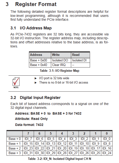
4.1 Isolated Digital Input Register (Read Only BASE+0~BASE+3)
4 consecutive 32-bit I/O addresses, with each bit corresponding to one IDI channel:
BASE+0 → IDI0‑IDI7
BASE+1 → IDI8‑IDI15
BASE+2 → IDI16‑IDI23
BASE+3 → IDI24‑IDI31
Bit=1 represents input high level, bit=0 represents input low level.
4.2 Isolated Digital Output Register (only write BASE+0~BASE+3)
4 consecutive 32-bit I/O addresses, with each bit corresponding to one IDO channel:
BASE+0 → IDO0‑IDI7
BASE+1 → IDO8‑IDI15
BASE+2 → IDO16‑IDI23
BASE+3 → IDO24‑IDI31
Bit=1 outputs conduction, bit=0 outputs shutdown.
4.3 Interruption Description
Only DI0 (INT1) and DI1 (INT2) channels are configurable interrupts; Support separate activation or simultaneous activation of two channels; There is no COS status change detection.
The BASE+0x40 write operation is used to clear the interrupt request flag bit.
Appendix A DOS/Windows Library API
A. 1. Basic data types
U8、I16、U16、I32、U32、F32、F64、Boolean。
A. 2 main API functions
Function Function Description
_7432Initial (DOS)/W_7432Initial (Win) initializes the board, scans and identifies the PCIe 7432 system, obtains the number of boards, base addresses, and interrupt numbers; Must be called first
_Read all 32 isolated DIs and return U32 values for 7432dI/W_7432dI
_7432dO/W_7432dO outputs 32-bit data to control all DO channels
_7432_Set-INT-Control/W_7432_Set-INT-Control Interrupt source control, enable/disable INT1 (DI0), INT2 (DI1)
_Read the interrupt status and determine whether DI0 or DI1 is causing the interrupt
W_7432/INT_Snable (Windows) Enable interrupt, bind Windows event handle
W-7432INT_Sisable (Windows) Close Interrupt (Win95 driver only)
Return error code: ERR_CoError is normal; ERR_SoardNoInit board not initialized; ERR_CCIBiosNotExist has no PCI BIOS.