ADLINK NuPRO-842 Full length PICMG 1.0 PCI/ISA Industrial Single Board Computer
Chapter 1 Product Overview (Hardware Platform, Core Specifications)
1.1 Standard Version Specifications
Full length PICMG 1.0 Rev1.0 (compatible with PCI+ISA dual bus), size 388mm × 122mm, suitable for traditional industrial full length chassis.
1.2 Computing Core Platform
CPU: MPGA478 slot, supports desktop Pentium 4/mobile Pentium 4-M processors, FSB 400/533MHz (jumper automatic/manual switching), maximum 3.06GHz desktop, 2.4GHz mobile CPU; Single processor, 512KB on-chip L2 cache, supports hyper threading, and comes with VRM9.0 power supply circuit
Chipset: Intel 845GV GMCH integrated graphics card Northbridge+Intel 82801DB ICH4 Southbridge+IT8888 PCI to ISA bridge
Memory: 2-channel 184 pin non ECC DDR DIMM slots, must be installed in pairs with the same specifications, maximum 2GB DDR266, dynamically shared memory for integrated graphics card
BIOS 4MB Phoenix Ward firmware, supports write protection, PXE diskless, DMI hardware information, USB boot, on-site BIOS refresh
1.3 Full board I/O resource list
display system
Onboard Intel Extreme Graphics integrated graphics card, 350MHz RAMDAC, rear DB15 VGA, up to 2048 × 2048 resolution 1536@32bit Reserved DVO digital display interface, can be paired with optional DB-842DVI daughter card output DVI/LVDS/TTL industrial LCD screen, with a maximum dynamic video memory of 64MB (only 32MB allocated when memory<256MB)
Internet
Dual Intel 82540EM Gigabit RJ45 Ethernet ports, PCI bus, supporting 10/100/1000M adaptive, IEEE802.3x flow control, WOL remote wake-up PXE, Each network port has an independent static MAC, with RJ45 built-in dual color speed/link indicator lights
Serial port COM
COM1 fixed RS232; COM2 can switch between RS232/RS422/RS485/485+four levels through multiple jumper wires, all of which are 10 pin onboard pins. The default addresses are COM1=3F8 IRQ4 and COM2=2F8 IRQ3
Parallel port
26 pin pin IEEE1284 parallel port, BIOS can choose Normal/EPP/ECP printing mode, default 378 IRQ7
USB
There are a total of 6 USB 2.0 ports (480Mbps): 1 rear panel, 5 onboard pins; Single port 5V/0.5A with overcurrent protection, compatible with USB1. x devices
Storage Controller
ICH4 integrates dual channel Ultra ATA100 IDE (primary/secondary channels, each channel supports two hard drives); W83627HF integrated standard 34 pin floppy drive controller
Expansion Slots
Mini PCI 32bit/33MHz slot, capable of external network card, storage, and acquisition daughter card
audio
AC’97 2.3 onboard pin, needs to be matched with an audio board for lead out
keyboard and mouse
Rear composite PS/2 circular interface (Y-line connected to keyboard and mouse simultaneously), additional onboard external keyboard pins
Hardware monitoring and watchdog
Winbond W83627HF SuperIO+W82782 monitoring chip: real-time acquisition of CPU temperature, board temperature, dual fan speed, and various DC voltages; Programmable watchdog WDT, timing 1-255 seconds/1-255 minutes, timeout machine hard reset, register records WDT reset fault flag
Chassis management pin
Front panel (power on/reset/power/hard disk light/beep/keyboard lock), chassis cover opening detection, two CPU fan sockets
1.4 Environment and Certification
Working temperature: 0-60 ℃ (forced air cooling for heat dissipation); Storage -40~85 ℃
Humidity of 5%~95% without condensation; Support vibration/shock industrial testing
Certification: CE, FCC A-level, UL-1950, CSA, VDE industrial safety certification
1.5 Operating System Support
Windows98/ME/NT4/2000/XP、RedHat Linux, Support various embedded real-time systems
Chapter 2 Connectors and Jumpers (Full Pin, DIP Configuration)
2.1 Motherboard layout
The drawings are fully labeled with CPU, 845GV North Bridge, ICH4 South Bridge, and Double DDR slots Mini PCI、 All onboard pins, jumpers, lithium batteries, and fan sockets are located to distinguish between exposed rear panels and internal pins.
2.2 Definition of all interface pins (standardized table)
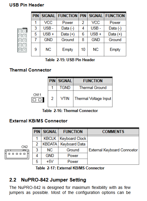
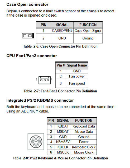
Includes VGA, RJ45 Gigabit, 10pin COM, 26pin parallel port, 34pin floppy drive, 40pin IDE, AC97 audio, USB plug PS/2、 External keyboard, fan, chassis cover, front panel, Mini PCI 124 pin complete pin signal, power supply, and ground wire definitions.
2.3 Key Function Jumper (Core Configuration Switch)
JP6 Clear CMOS: Short circuit 2-3 pins when powered off, clear RTC time, BIOS settings, power on password
JP8 FSB frequency selection: 1-2 automatic detection, 2-3 forced 400MHz, suspended forced 533MHz
JP1/JP2/JP3 COM2 level switching: combination jumper switching RS232/422/485
JP4 RS485+mode specific jumper, compatible with bus devices with automatic transmission and reception control
Chapter 3: Step by Step Tutorial for Hardware Installation
Pre installed mandatory anti-static requirements
Anti static workbench and grounding wristband throughout the process. It is forbidden to touch CPU/memory gold fingers with bare hands, as static electricity will permanently burn components.
3.1 CPU installation
Unlock the mPGA47 slot lock rod and remove the protective cover; CPU Triangle Mark Alignment Slot Pin1
The CPU is placed flat without external pressure, and the locking rod makes a clicking sound
Apply thermal grease evenly to the CPU core, lock the original heat dissipation module, and connect the fan to the FAN socket; Without heat dissipation, it will overheat, shut down, and burn out
3.2 DDR Memory Installation
DIMM1+DIMM2 must be inserted in pairs with the same specifications, and the slot buckle will automatically lock; Single memory cannot boot up properly, supports 64MB~1GB single DDR266
3.3 IDE hard drive wiring
Distinguish between primary/secondary IDE channels, align the motherboard and hard drive pins with the red Pin1 ribbon cable, and mount up to two IDE devices (primary/secondary) per channel
3.4 Basic BIOS Operations
Press Del to enter the Phoenix Ward settings interface during power on self-test, where you can adjust the startup sequence, serial port mode, parallel port type, WDT switch, power management, and hardware monitoring threshold; Parameters are stored in the lithium battery RTC
3.5 Key points of operating system installation
BIOS prioritizes setting CD/floppy drive startup; Before installing the system, load the original chipset driver and identify all PCI/ISA hardware
Chapter 4: Device Driver Installation (Windows Full Process)
The drivers are stored uniformly on the accompanying ADLINK CD, divided into three categories: chipset, graphics card, and network card. They support Win98/ME/NT/2000/XP and have a fixed installation sequence:
Intel 845GV chipset INF driver: Low level bus recognition, close background program to run Setup, restart after installation
Integrated graphics card driver: separate installation packages for Win9X/NT/2000/XP, covering 2D acceleration and multi display output
Intel 82540EM Gigabit Network Card Driver: Automatically batch recognizes dual network ports, supports WOL and PXE functions
The CD comes with the source code for watchdog testing under DOS, which can be used for secondary development of industrial control programs
Chapter 5 Development Instructions for Watchdog Timer WDT
Hardware architecture: Integrated on board programmable logic devices, two-level countdown, IO port 02E/02F control
Work logic: The software periodically executes the “feed dog” refresh timer; Trigger hardware reset of the entire machine after timeout
Two timing modes: second level (1-255s), minute level (1-255min)
Fault tracing: After the system restarts, the registers can be read to determine whether the restart was triggered by a watchdog
Development Resources: The CD provides complete DOS sample C code, which can be ported to Windows industrial control programs
Chapter 6: Optional DB-842DVI Digital Display Subcard
6.1 Functional positioning
NuPRO-842 dedicated expansion daughter card, connected to the motherboard DVO digital display interface, simultaneously outputs three types of industrial display signals: DVI, LVDS, TTL, supporting 800 × 600/1024 × 768@60Hz Industrial resolution.
6.2 Chip Architecture
Chronotel CH7301 (DVI encoding)+DS90C387 LVDS transmitter+matching TTL conversion chip
6.3 Sub card jumper configuration
JP1: LCD screen power supply selection 3.3V/5V
JP2: LVDS output enabled/disabled
6.4 Interface pins
Complete DVI (CN1), LVDS (CN2), and TTL (CN3) panel connectors with all signal, power, and ground definitions table
Additional chapter: Safety regulations and global after-sales service
Safety operation terms
Before disassembly, completely cut off the power, stay away from liquids, high temperatures, and blocked ventilation vents
The replacement model of the CR2032 lithium battery on the motherboard is incorrect and there is a risk of explosion. The waste battery is being recycled in compliance with regulations
Private disassembly, water ingress, incorrect voltage, and physical impact are not covered by the warranty