ADLINK PCI-7200/cPCI-7200 high-speed digital I/O board
Product Overview
1. Differentiation between two models
PCI-7200: Standard 32-bit PCI bus industrial DIO card;
CPCI-7200: The specifications of the 3U CompactPCI industrial control chassis are consistent with the main functions, with an additional 4 auxiliary DI/DO channels, a larger 2K input FIFO, and a 100pin interface;
The underlying registers and driver APIs of the two are completely universal, and unless otherwise specified in the documentation, they are collectively referred to as PCI-7200.
2. Core positioning
32 TTL bidirectional digital IO channels, supporting 12MB/s bus main control DMA high-speed transmission, built-in 8254 timing counter, hardware handshake, internal and external triggering, suitable for high-speed digital pattern generators, external AD/DA synchronization, peripheral high-speed interfaces, BCD devices, pulse waveform output scenarios.
3. Core Highlights
32DI+32DO full TTL level, bus master DMA does not require CPU usage;
Maximum throughput of 12MB/s, built-in hardware FIFO buffer;
8254 three channel programmable timer, generating 0.00046Hz~2MHz sampling clock;
Four working modes: direct read/write, internal timing, external triggering, hardware handshake;
Interrupt, overflow/underflow hardware status detection;
DOS, Win95 dual platform C library+Windows DLL, supporting testing tool 7200UTIL.
Hardware electrical and specification parameters
1. Digital IO electrical (TTL compatible)
Input: Low level ≤ 0.8V, high level ≥ 2.0V; Input load low charging 0.6mA, high pulling 20 μ A;
Output: Low maximum 0.5V, high minimum 2.7V; irrigation current 24mA, pulling current 3mA, strong driving capability;
Auxiliary AUX I/O (cPCI-7200 only): 4DI+4TTL DO.
2. FIFO cache configuration
PCI-7200: 32 word (32-bit) on-chip FIFO for DI/DO;
CPCI-7200: on-chip 32 word+additional 2K depth DI FIFO, supports full/empty hardware flags.
3. 8254 timer counter (global clock 4MHz)
3 independent 16 bit counters Timer0/1/2:
Timer0: Sampling cycle of digital input;
Timer1: Digital output update rhythm;
Timer2: Can be cascaded with 0/1 and extended to extremely low frequencies;
Frequency division formula: Single timer 4MHz/division value, cascaded 4MHz/(Cx * C2), output range 0.00046Hz~2MHz.
4. Machinery, power supply, and environment
PCI-7200: size 98 × 147mm, power supply+5V 500mA, CN1 (40pin ribbon cable)+CN2 (37pin D-Sub) dual interface;
CPCI-7200: Standard 3U cPCI, power supply+5V 600mA, single 100pin SCSI interface;
Environment: Working at 0-50 ℃, storage at -20~80 ℃, humidity at 5-95%, no condensation.
5. Interface signal definition
Universal control signal (both models have):
I-TRG external input trigger, I-REQ input request, I-ACK input response;
OTR external output trigger, OREQ output request, OACK output response;
Handshake logic: REQ notifies external, ACK feedback board completes.
Key points of hardware installation chapter
Plug and play design: no dip/jumper, IRQ and I/O base addresses are automatically allocated by BIOS;
Installation requirements for static electricity: anti-static pad, anti-static wristband, check the chip before powering on;
Supporting cables: PCI version comes with a 40 to 37 pin cable; CPCI with 100 pin SCSI wiring harness;
Windows 95 driver installation process: A new device window pops up on the hardware, and the VXD driver is loaded on the specified CD X: \ Software \ 7200 \ Win95 path;
Test tool 7200UTIL.EXE: DOS/Windows dual end, capable of polling DIO, DMA mode, cPCI assisted IO function verification, automatically reading board card base address and interrupt number.
Interface pins:
PCI CN2(37pin):DI0~15、DO0~15、I_TRG/I_REQ/I_ACK;
PCI CN1(40pin):DI16~31、DO16~31、O_TRG/O_REQ/O_ACK;
CPCI 100 pin integrates all 32DI, 32DO, 4AUXD, 4AUXD, and all handshake trigger signals.
Register structure (core underlying operations)
The board occupies a continuous 32-bit I/O port, and cPCI adds an AUX register. Key registers:
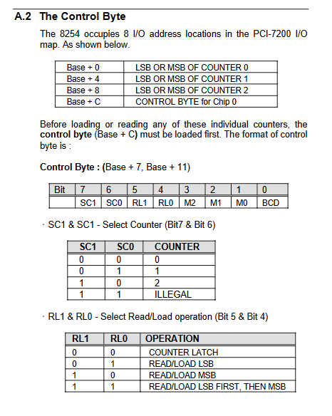
Read and write three counters: Base+0/Counter0~Base+8/Counter2: 8254;
Base+C: 8254 control word register;
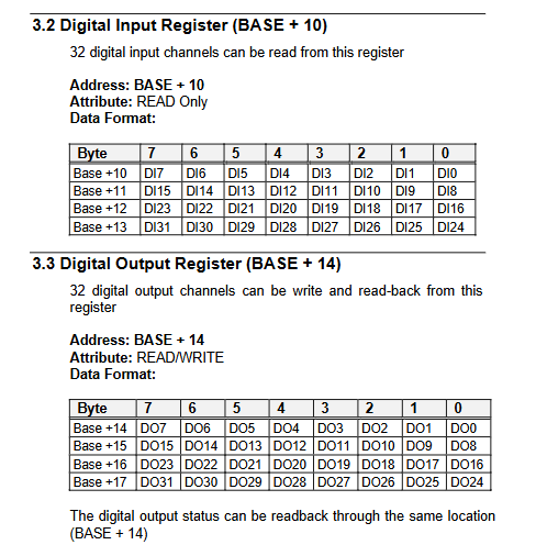
Base+10: Read only 32-bit digital input register;
Base+14: Readable and writable 32-bit digital output register (supports read back);
Base+18: DIO status control register (FIFO enable, trigger polarity, handshake switch, overflow/underflow flag);
Base+1C: Interrupt control/status register (I2REQ, OACK, timer interrupt enable and status bit);
CPCI Exclusive Base+20: Auxiliary DI/DO Register.
Key status position:
I-OVR: Input F overflow; ○UND: Output F underflow; Setting 1 requires software reset;
Interrupt source: Timer 0/1/2, I-REQ, O-ACK can be optionally enabled.
Four core working modes (Chapter 4 Working Principles)
1. Direct program control (polling mode)
The CPU directly reads and writes the Base+10/Base+14 registers, with a single read and write of all 32 channels, suitable for low-speed and low bit control.
2. Internal timer Pacer DMA mode
8254 generates a fixed beat, automatically locks DI/updates DO at the scheduled time, and transfers batch data to the system memory through the PCI bus main control DMA. The background automatically transfers the data, and the CPU only processes the entire block of data.
3. External I-REQ triggers DMA mode
External devices use hardware pulse locking DI through I-REQ, while the rest of the logic is synchronized with timing DMA for external AD/DA synchronous acquisition.
4. REQ/ACK hardware handshake mode
Bidirectional hardware response, board and external device synchronization:
Input process: Send an external I-REQ → Lock data on the board → Return an I-ACK;
Output process: DMA loads DO → board sends OREQ → receives OACK and refreshes the next group;
The only transmission mode that can guarantee 12MB/s without loss, preferred for high-speed scenarios.
Time sequence specification
The manual provides the minimum holding time for high and low levels of the I-REQ, O-REQ, handshake signal, and establishes/holds timing parameters. Hardware docking must meet the timing requirements.
Software Development Library (Chapter 5 C/DLL Complete API)
1. Platform differentiation
DOS: Pure C static library, function prefix _7200_;
Win95/98: DLL driver, function prefix W_7200_;
Support mainstream development tools such as VC, VB, Borland C, Delphi, etc.
2. Classification of API Functions
Board management
_7200Initialize the board, read the base address/interrupt; _7200_Switch_Card_Co multi card switching (up to 4 PCI-7200 cards);
Basic DI/DO Reading and Writing
Batch 32 channel read-write _7200-DI/_7200-DO; Single point read-write _7200-DI_Channel/_7200_DO_Channel;
CPCI exclusive auxiliary IO
_7200_ AUX DI/_ 7200_ AUX DO Batch/Single Channel 4-channel Auxiliary IO;
DMA memory management (exclusive to Windows)
Alloc_DMA_Mem single buffer, Alloc_DBDMA_Mem double loop buffer; Supporting the release of memory function;
DMA acquisition control
DI-DMA_Start starts input DMA and supports three types of triggers: timed/external/handshake; DI_SMA_Status query progress; DI_SMA_Stop stops;
DO_SMA_Start outputs DMA and supports timing/handshake;
Double buffer dedicated function
DblBufferMode enables loop buffering; CheckHalfReady half area data readiness judgment; DblBufferTransfer copies half of the data; GetOverrunStatus counts the number of overflow occurrences;
Timer configuration
DI_Timer configuration input frequency division; DO_Timer configuration output frequency division, supports single/cascade mode.
3. General programming process
Initialize board → Configure timer/trigger mode → Allocate DMA memory (high-speed scenario) → Start DMA transfer → Loop read/process data → Stop DMA and release memory.
Double Buffer DMA Principle (Chapter 6)
Only digital input supports circular double buffering:
The memory logic is divided into two equal half buffers;
Fill the first half of the hardware and switch to the second half after filling;
The application can synchronously read the filled half area, achieving uninterrupted continuous collection without data loss;
If the upper layer fails to read in a timely manner, overflow may occur, and the interface can be called to count the number of overflow occurrences.
Three major limitations on hardware usage (Chapter 7)
The theoretical peak of 12MB/s can only be achieved when a single PCI device monopolizes the bus, and the bandwidth decreases when multiple PCI devices coexist;
In internal/external triggering mode, due to limitations in FIFO depth and PCI bus delay, high-speed data integrity cannot be guaranteed, and only handshake mode stabilizes at 12MB/s;
The maximum single DMA transfer is 64MB (2 ^ 26 bytes), exceeding which segmented processing is required.
Appendix A: 8254 Timer Complete Information
3 independent 16 bit counters, 6 working modes (interrupt counting, monostable, rate generator, square wave, software/hardware gating pulse);
Control byte SC counter selection, RL read-write format, M working mode, BCD binary switching;
Timing and counting range of each mode (binary 0~65535, BCD 0~9999), used as a reference for timing beat generation.
Supporting tools, system support, and warranty
Supporting software: 7200UTIL testing tool, DOS C library Win95 DLL、 Example program;
Third party compatibility: LabVIEW and HP-VEE can be integrated through drivers;
Warranty: Original factory 1-year hardware warranty, no warranty for human modification or use beyond specifications.