ADLINK PCI-9812/PCI-9810 synchronous 4-channel high-speed acquisition card
Product Overview
1. Core differences between the two models
PCI-9812:12bit ADC resolution;
PCI-9810:10 bit ADC resolution;
The hardware channel, clock, trigger, interface, and mechanical dimensions are completely consistent, except for the ADC sampling accuracy.
2. Core positioning
4-channel synchronous single ended analog acquisition card, capable of up to 20MS/s single channel sampling, equipped with onboard 32K sampling FIFO+PCI bus main control DMA, specially designed for high bandwidth transient signal scenarios such as RF acquisition, ultrasound imaging, CCD video digitization, vibration testing, instrument signal acquisition, etc.
3. Core hardware highlights
Four independent ADCs, hardware synchronous sampling, no phase shift between channels;
Maximum 20MHz sampling rate, supporting three types of clock sources: internal/external sine/digital;
Weldable configuration input impedance (50 Ω/1.25k Ω/15M Ω) and dual range of ± 1V/± 5V;
5 types of trigger modes, multiple trigger sources (software/analog level/external digital edge);
32K sample board mounted FIFO alleviates PCI bandwidth bottleneck, bus master controls DMA with zero CPU handling;
Supporting DOS/Win95 development library and visual 9812UTIL calibration testing tool;
Complete hardware and electrical specifications
1. Analog input AI (4-channel synchronous single ended)
ADC chip: BB ADS800 series;
Resolution: PCI-9812 12 12 bit, PCI-9810 10 bit;
Input range (PCB pad selection): Bipolar ± 1V/± 5V;
Optional input impedance (CxLO/Cx5V independent pads per channel):
Open circuit LO, open circuit 5V: 15M Ω, only compatible with ± 1V;
Open circuit LO, short circuit 5V: 1.25k Ω, only compatible with ± 5V;
Short circuit LO, open circuit 5V: 50 Ω (default), compatible with ± 1V;
Short circuit LO, short circuit 5V: 50 Ω, compatible with ± 5V;
Note that the high impedance mode input terminal must be connected to a signal source, otherwise charge accumulation can damage the ADC;
Linear error: 25 ℃ typical DNL ± 0.4LSB, INL ± 1.9LSB; Gain error ± 1.5% FS;
Sampling rate rule:
Only CH0 enabled: maximum 20MS/s, FIFO total 32K;
CHO+CH1 dual channel: up to 20MS/s, with 16K FIFO allocated for each channel;
Four channels fully open: up to 20MS/s, with only 8K FIFO per channel;
Exceeding the FIFO capacity may result in data overflow and disconnection.
2. Clock system
Onboard reference 40MHz internal clock, divided and output ADC sampling clock;
The frequency divider has an even range of 2~1024, with a sampling rate of 40MHz per division value;
Three types of external clock inputs:
J5 BNC external sine clock (50 Ω impedance, 2V peak to peak AC coupling);
JP1 pin external digital square wave clock (DC coupled 50 Ω, 2.4~5V level);
The external clock frequency must be ≥ 2 times the target sampling rate;
3. Trigger the system
5 trigger modes: software trigger, post trigger, pre trigger, intermediate trigger, delayed trigger;
Pre triggering: data collection first, external triggering arrives and stops;
Post trigger: Collection only starts after triggering;
Intermediate trigger: Collect data before and after triggering;
Delay triggering: After triggering, delay the collection of specified samples;
trigger source
Software trigger: Call API to start directly;
Simulation trigger: Any channel from CH4 to CH4 can be set with 8-bit level threshold and rising/falling edge;
External digital trigger: JP1 pin edge trigger;
16 bit post counter, used for delay/post sample counting control;
4. Digital input (JP1 10 pin row)
1 external digital clock, 1 external digital trigger, 3 universal TTL DI;
Internal 10K pull-down resistor, low level ≤ 0.8V, high ≥ 2.0V;
5. Machinery, power supply, and environment
Size: 101mm (H) × 173mm (L) standard PCI short card;
Power supply:+5V, maximum 2.5A;
Working temperature: 0-40 ℃, storage: -20-80 ℃, humidity: 5-85%, no condensation;
6. Connector layout
5-way BNC rear interface: CHO/CH1/CH2/CH3 analog input, external sine clock J5;
Onboard JP1 10pin pin: digital clock, digital trigger, 3-channel DI, all GND;
Hardware installation and anti-static specifications
PCI plug and play design, no jumper/dip code, IRQ and I/O base addresses are automatically allocated by BIOS;
The simulation range and input impedance must be set through PCB copper pad short circuit, and cannot be modified by software;
Installation steps: power-off disassembly, static discharge, insertion into 32-bit PCI slot, fixing baffle;
Win95 driver installation: Select the manufacturer’s disk in the new hardware pop-up window, path X: \ Software \ PCic_Card \ 9812 \ Win95 to load VXD driver;
Supporting materials: collection card body, 5 BNC terminals, software manual CD;
Bottom level I/O register structure (10 sets of 32-bit base address registers in total)
All registers have 32-bit read and write capabilities, with access to 8/16 bits prohibited. Key register functions include:
BASE+0 channel enable register: bits 0-3 control CHO~CH3 switches, only allowing single/double (CHO+1)/four channel combinations;
BASE+4 clock division register: 16 bit even division value 2~1024;
BASE+8 trigger mode register: 3-bit encoding for 5 acquisition modes;
BASE+C trigger level register: 8-bit corresponds to ± 1V/± 5V threshold voltage;
BASE+10 trigger source register: select analog channel/external digital, rising/falling edge;
BASE+14 post 16 bit counting register;
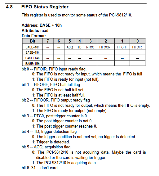
BASE+18 FIFO status/control register: half full, overflow, collection run, trigger detection flag, supports clearing FIFO/trigger flag;
BASE+1C acquisition enable bit: global switch ADC conversion;
BASE+20 clock source register: Switch between internal/external sine/external digital clock to distinguish clock above/below PCI 33MHz.
Working principle of collection
1. ADC conversion process
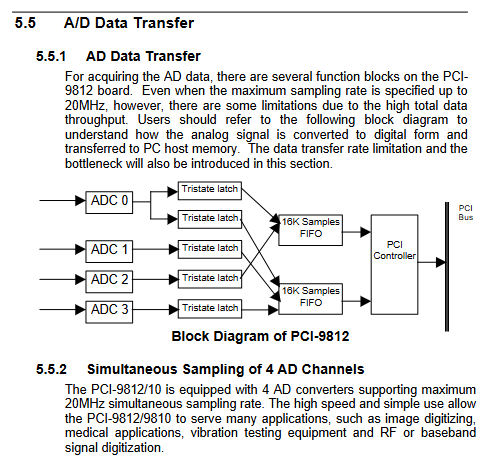
Four ADC synchronous pipeline conversion, sampling data stored in two-stage 16K onboard FIFO, and then directly transferred to the host continuous memory by AMCC S5933 PCI main control DMA, with the CPU only performing data post-processing.
2. Bandwidth and FIFO limitations (key usage constraints)
The maximum throughput of a single channel is 20MS × 2Byte=40MB/s, and the total throughput of all four channels is 160MB/s, far exceeding the theoretical 132MB/s bandwidth of 33MHz PCI
Total throughput>PCI continuous bandwidth: The collection length is limited by FIFO (4-channel 8K samples, dual channel 16K samples);
Total throughput<PCI bandwidth: The maximum length of a single acquisition is limited by the 64MB address of the PCI controller;
Continuous unlimited collection requires a dual buffering software mechanism, and the CPU hard disk write speed cannot be lower than the data stream;
3. Multi card synchronization limitations
Multi card shared external clock can only achieve half a sampling cycle error and cannot be fully synchronized with hardware;
4. AD data encoding rules
PCI-9812 (12 bits): The valid data occupies 16 bits, with the high 12 bits being invalid and the low 4 bits being invalid. The voltage conversion formula is voltage=sampled value/32752 × range;
PCI-9810 (10 bits): Effective data occupies 16 bits, with the top 10 bits being invalid and the bottom 6 bits being invalid. Voltage=sampled value/32704 × range.
C/C++high-level development library
1. Platform differentiation
DOS: Function prefix _9812_, Borland C static library;
Win95: DLL driver, prefix W-9812_, supports VB/VC/Delphi;
2. List of core API functions
_9812Initialize: Initialize the specified card number (0-9) and read the base address/IRQ;
_9812_Close: Release board resources;
_9812_Set_Clk_Src: Select internal/external sine/external digital clock;
_9812_Set_Clk-Rate: Configure the frequency division value;
_9812_Set_Trig: One stop configuration for trigger mode, source, edge, level, and post count;
Windows specific memory interface: W-9812_Salloc_DMA_Sem allocates continuous DMA memory, W-9812_Sree_SMA_Sem releases;
DMA acquisition control: Start background acquisition, query progress, and terminate acquisition;
W_9812_Set_Sample: VB and other pointer free languages read buffer samples;
3. Standard programming process
Initialize the board → Configure channels/clocks/triggers → Allocate DMA memory → Start DMA acquisition → Read data in a loop → Stop acquisition, release memory, and shut down the board.
Hardware Calibration Chapter
Calibration tool requirements: high-precision DC standard source, supporting 9812UTIL calibration program;
PCB adjustable potentiometer VR allocation: VR1~VR4 correspond to 4-channel offset calibration, VR5~VR8 correspond to 4-channel full amplitude gain calibration;
Calibration steps (single channel as an example):
Input full DC and adjust the gain VR to a reading error of ≤± 0.1;
Input 0V and adjust the offset VR to a reading close to 0;
Repetitive iteration of gain+offset;
Calibration cycle: 6-12 months in the laboratory, and it is recommended to recalibrate after 3 months for temperature changes/vibration environments; Pre calibrated at the factory.
Supporting upper level tool 9812UTIL.EXE
Menu based visualization tool under DOS, with three core functions:
System configuration: View card number, clock, trigger, range hardware configuration;
Calibration function: guide step-by-step adjustment of VR potentiometer, real-time display of sampling mean;
Function testing: Real time waveform drawing, switchable trigger mode, trigger level, channel number, intuitive verification of acquisition function, built-in waveform display interface.
Full platform software ecosystem
Bottom layer: DOS C library, Win95 DLL, NT system PCIS-DASK driver package;
Configuration/testing software: DAQBench ActiveX control, LabVIEW VI driver, DASYLab rapid testing software;
Typical application scenarios
RF/baseband signal digitization, ultrasound medical imaging, gamma camera, CCD video acquisition, high-speed instrument testing, vibration and shock transient signal capture.