ADLINK PXIe-9529H is an 8-channel 24 bit, 256kS/s synchronous sampling dynamic signal acquisition PXIe module
Product Overview and Core Features
Main hardware features
1. Analog input: 8-channel synchronous sampling, 24 bit ∑ – Δ ADC; Sampling rate of 8kS/s to 256kS/s; The maximum dynamic range is 105dB.
2. Coupling method: The software can choose AC/DC coupling; AC coupled high pass cutoff -3dB point * * 0.3Hz * *, suitable for vibration and acceleration signals.
3. IEPE Incentive: Each channel software can be configured with * * 4mA constant current excitation * *, with a maximum compliant voltage of 24V; turning on IEPE will automatically switch to AC coupling, compatible with accelerometers and microphones.
4. Input mode: differential/pseudo differential; Input range: * * ± 1V, ± 10V * *.
5. Onboard automatic calibration: Equipped with a reference source, it can self calibrate without the need for an external signal source; The calibration constants are stored in the onboard EEPROM.
6. Interface panel: 8-channel analog input SMB; One external number triggers SMB.
Typical Applications
-NVH noise, vibration, and roughness testing
-Structural Health Monitoring SHM
-Phased array data acquisition
-Equipment status monitoring
Software support (MAPS software ecosystem)
All drivers and tools can be downloaded from Linghua’s official website, and commercial drivers require an authorization code; Unauthorized access to 2-hour demo version.
1. MAPS Core (must be installed)
-ACE (ADLINK Connection Explorer) Device Manager: Identify hardware, set DMA buffers, set device aliases; Built in Soft Front Panel, directly GUI collects waveforms.
-PXI platform resource management, ChassisWatch, DAQ module functional testing tools.
2. MAPS/C: C/C++development library, header files API、 Example code.
3. MAPS/LV: LabVIEW driver and examples.
4. PCIe Geni x4 bus; DMA supports scatter gather, supports non contiguous system memory, and enables long-term continuous streaming of disks; Single block transmission without aggregation can reach a maximum of 8MB; after enabling aggregation, it is only limited by the system’s physical memory.
Installation operation
Static sensitive devices must be operated with anti-static wristbands and pads.
1. Power off the PXI chassis power supply before installation.
2. Align the module with the slot rail of the chassis and push it in. Tighten the pop-up handle until you hear a “click” on the buckle, and then tighten the panel screws.
3. When powered on, Windows recognizes hardware through MAPS Core.
4. Packaging List: Only the PXIe-9529H module body.
Key electrical specifications
Analog input
|Project | Parameters|
|Channel | 8-channel synchronization, 24 bit|
|Sampling rate | 8kS/s~256kS/s|
|Range | ± 1 V, ± 10 V|
|Input Mode | Differential/Pseudo Differential|
|Input impedance | Differential: 1M Ω positive and negative respectively; Pseudo differential negative terminal 50 Ω|
|AC coupling cutoff | 0.3 Hz (-3dB)|
|IEPE incentive | 4 mA/channel, compliant voltage 24V|
|Overvoltage protection | Differential ± 42.4V; Pseudo differential positive terminal ± 42.4V, negative terminal only ± 2.5V without protection|
|Misalignment error | Maximum ± 0.2 mV|
|Gain error | Maximum ± 0.05%|
|Background noise | 40 μ Vrms @ 256kS/s|
|SNR signal-to-noise ratio | ± 1V: 91dB; ±10V:93dB @256kS/s |
|THD total harmonic distortion | ± 1V: -118dB; ±10V:‑113dB @256kS/s |
|Dynamic range | ± 1V: 104dB; ±10V:105dB @256kS/s |
|Crosstalk | -105 dB (Rev1.1 update)|
Time base
-Sampling clock: onboard 10MHz crystal oscillator; PXIe backplane 10MHz external reference can also be used;
-Delay trigger time base: 125 MHz.
Trigger the system
1. Trigger source: software trigger, analog channel trigger, external digital SMB trigger, PXI STAR, PXIe-DSTARB, PXI trigger bus TRIG0-TRIG7.
2. External digital trigger: TTL5V level; Support rising/falling edges; The minimum pulse width is ≥ 10ns.
3. Trigger the working mode
-Post Trigger: After the trigger arrives, collect the set point count;
-Delay Trigger: After triggering an event, wait for a programmable delay before starting data collection; The minimum delay is 8ns, and the maximum is determined by a 32-bit counter;
-Re Trigger: Multiple triggering events, with each trigger collecting a set of data, automatically processed by hardware without software intervention.
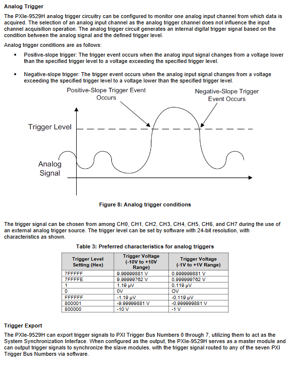
4. Simulation trigger: Any one of the 8 channels can be selected as the trigger source; Positive/negative slope can be set, and trigger level can be set for 24 bit resolution.
5. Trigger output: Internal trigger events can be output to PXI trigger bus 0-7 for multi card synchronization.
Machinery and Environment
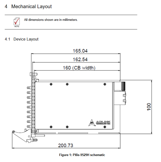
-Size: 160mm (board width) × 100mm (board height);
-Working temperature: 0 ℃~55 ℃; Storage -20 ℃ to 80 ℃;
-Humidity: 10-90% without condensation;
-Certification: CE, FCC Class A.
Hardware working principle
Simulate front-end architecture
1. Differential mode: Suitable for grounding reference signals and suppressing common mode noise;
2. Pseudo differential mode: suitable for floating ground signals, with the negative terminal connected to the reference ground through 50 Ω to prevent common mode drift;
3. AC coupling: internal RC high pass, filtering out DC components; Automatically switch AC when IEPE is enabled; DC coupling retains DC component.
4. PGA programmable gain amplifier, followed by a 24 bit ∑ – Δ ADC.
5. Onboard FIFO cache ADC data, PCIe bus DMA transfer to host memory; Support circular multi buffer DMA to achieve continuous acquisition.
Multi module synchronization SSI (System Synchronization Interface)
By relying on the PXI Trigger Bus [0-7] on the PXI backplane, multi card synchronization can be achieved without the need for external cables
1. Master card: generates triggers/clocks and outputs them to a certain PXI trigger bus; Use a backplane of 10MHz as the time base;
2. Slave from the card: configure the trigger source to correspond to the PXI trigger bus and receive the main card signal;
Note: Different functional signals cannot be multiplexed onto the same PXI trigger bus.
Appendix A: Calibration Mechanism
The module has been calibrated at the factory, and the calibration parameters are burned into the onboard EEPROM, which is divided into two storage areas:
Bank0 (factory area): write protect, save factory calibration constants; The driver defaults to loading Bank0 first.
Bank1 (User Area): Save the user’s automatic calibration results.
Auto Calibration Automatic Calibration
No need for external standard source, use onboard reference voltage to eliminate gain and offset errors caused by temperature drift and time drift.
Operation suggestion: Preheat the module when powered on for at least 20 minutes; Disconnect the external input cable and perform automatic calibration again.
-The API can switch between loading Bank0 or Bank1 after startup, and the settings will be permanently saved in EEPROM.