ADLINK PXI-3920/PXI-3910 3U PXI System Controller
Chapter 1 Product Introduction (Product Positioning and Core Features)
1. Product positioning
Both are 3U single slot PXI system controllers (system slot controllers), compatible with PXI Rev2.2 specifications, used for PXI hybrid testing platforms (PXI board+desktop GPIB/LXI instrument joint measurement and control); Full board CPU and memory chip soldering, no plug-in chips, paired with copper aluminum composite heat sink, earthquake and impact resistant, suitable for industrial, automotive, and production line testing environments.
2. Differences in core hardware between the two models
Parameter PXI-3920 PXI-3910
CPU Pentium M 760 2.0GHz, 2MB L2 cache, 533MHz frontend bus Celeron M 373 1.0GHz, 512KB L2 cache, 400MHz frontend bus
Power consumption of the whole machine 3.3V 1500mA/5V 7580mA/12V 550mA 3.3V 1480mA/5V 5050mA/12V 512mA
Same basic configuration 915GME+ICH6-M chipset, onboard 512MB soldered DDR2, 1 SO-DIMM expansion slot (maximum total 1.5GB); Standard 2.5-inch 80GB SATA hard drive, Type-II CF solid-state slot
3. Unify the core functions of the entire machine
Instrument control interface: onboard GPIB (IEEE488), dual gigabit network (one LAN, one LXI instrument specific), dual multifunctional serial ports;
Display: DVI-V composite interface (digital DVI+analog VGA), rear 18 bit LVDS screen output;
Peripherals: 4-channel USB 2.0, HD audio input/output, standard PXI backplane trigger bus;
Industrial control reliability: programmable hardware watchdog, full interface optoelectronic/electrostatic protection;
Dual storage solution: Standard SATA mechanical hard drive, supporting CF card replacement for hard drives (in high vibration scenarios).
4. Environment and Certification
Working temperature: 0-55 ℃, storage: -20~80 ℃; Humidity of 5%~95% without condensation;
Vibration: Run 0.5Grms with hard drive and 6Grms with solid-state drive; Impact 30G half sine pulse;
Electromagnetic compatibility CE Class A, compliant with the EN 61326 standard for industrial testing equipment.
5. Support for operating systems
Windows2000 / Windows XP / Windows Vista; Other systems can apply for adaptation from the original factory.
Chapter 2 Hardware Information (Block Diagram, Panel, Onboard Jumper, Storage)
2.1 Hardware Architecture Block Diagram
The motherboard is centered around the 915GME North Bridge and ICH6-M South Bridge, and is divided into five major pathways:
CPU+DR2 memory path;
Display channel: GMA900 integrated graphics card → DVI-I panel+rear LVDS;
Peripheral bus: PCIe dual gigabit network card, PCI bus GPIB, LPC super IO (dual serial port), HD sound card;
PXI backplane: J1 standard PCI bus, J2 PXI dedicated trigger bus, independent trigger control chip;
Storage: SATA hard drive, Type-II CF card, two independent storage channels.
2.2 All interfaces and indicator lights on the front panel
List of panel interfaces
SMB trigger port (TRIG): external PXI synchronous trigger signal;
DVI-I: Digital/Analog Display Output, Comes with DVI to VGA Adapter;
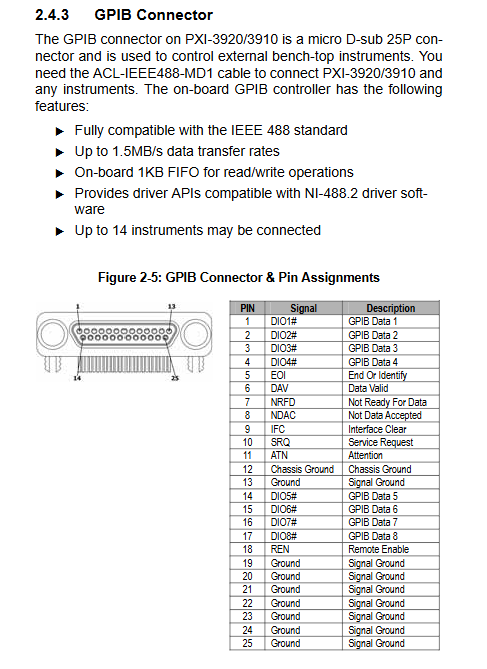
Micro DSUB25 GPIB: external desktop testing instrument, up to 1.5MB/s, can connect up to 14 instruments in series;
Reset small hole: hardware machine hard reset;
DB9 COM1/COM2 dual serial ports: jumper switch RS232/422/485;
4-channel USB 2.0 A port;
Dual RJ45 Gigabit Ethernet (speed dual color chain street light);
Audio dual jack: line input/headphone output.
Four sets of status LEDs
Green power light: always on when powered on;
Yellow hard drive light: SATA/CF read-write flashing;
Red watchdog light: The watchdog lights up after timeout;
Blue system health light: normally on, continuously flashing due to malfunction (abnormal needs to clear CMOS and restart).
2.3 Onboard Internal Connectors (PCB Bottom Layer)
Type-II CF slot: supports ATA/PIO mode and can replace hard drives as boot disks;
SATA Gen1 hard drive interface: 150MB/s bandwidth, supports 2.5-inch SSD/mechanical drive;
PXI J1: Standard 32-bit PCI bus backplane pins;
PXI J2: Dedicated 8-way PXI trigger bus (TRIG0~TRIG7).
2.4 Jumper configuration (core hardware settings)
JP9 (Clear CMOS): 1-2 short circuit is normal, 2-3 short circuit clears BIOS parameters, used for power on fault repair;
JP1~JP6 (COM1/COM2 mode): Configure two sets of serial port level standards respectively, with three options for RS232/RS422/485485 mode and built-in terminal matching.
2.5 Definition of Electrical and Interface Pins
The manual fully includes all pin signal definitions for DVI, GPIB, serial port, Ethernet port, CF, SATA, PXI J1/J2, distinguishing differential, power, ground, and control signal lines, and clarifying the requirements for external wiring current limiting resistors.
Chapter 3 Installation, Storage Replacement, and BIOS System Deployment
3.1 Pre installation requirements
Anti static specifications: Anti static wristband+anti-static pad, prohibit touching the board chip with bare hands;
Compatible chassis list: Supports PXIS-2506/2508/2558T-B/2630/2700 and NI full range PXI chassis; Prohibit old models such as PXIS-2556 and 2650;
PXIS-2558T-B Special Adaptation: Comes with an 8.4-inch rear LCD, BIOS requires Boot Display=CRT+LVDS, resolution 800 × 600.
3.2 Standard Packing Accessories
Main control card body, DVI to VGA connector, USB to PS2 adapter cable, user manual, driver CD.
3.3 Hardware disassembly and assembly steps
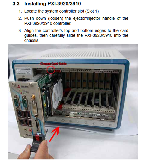
Insert the No.1 system slot into the chassis, and tighten the screws of the upper and lower locking buckles to lock the panel;
SATA hard drive replacement: Remove the four fixing screws on the back of the PCB, plug and unplug the onboard SATA cable, compatible with 2.5-inch SSDs;
CF card installation: The slot below the hard drive can be directly plugged and unplugged, and can coexist with SATA. BIOS switches the boot sequence.
3.4 BIOS and Startup Settings
Press Del to enter Phoenix Ward BIOS during startup. Core startup configuration:
Default first boot: SATA hard drive;
Optional boot media: CF card, USB optical drive, USB flash drive, USB portable hard drive, USB floppy drive;
Fault repair: When the system blue screen/cannot boot up, JP9 clears the CMOS and restores the factory BIOS.
3.5 Operating System Installation Process
Insert the corresponding USB boot medium and modify the first boot option in BIOS;
After completing the system installation, restart and switch back to the hard drive for priority boot;
After the system installation is completed, the complete set of original drivers must be installed in sequence.
Chapter 4: Complete Driver Installation Guide (Windows Platform)
The driver discs are divided into 7 categories and must be installed in order, with each step completing a restart:
Chipset driver: 915GME/ICH6 motherboard underlying bus, SATA/USB/PCIe support;
Graphics card driver: Intel GMA900 integrated display, PXIS-2558T-B requires dual display mode to be enabled;
Dual Gigabit Network Card Driver: Marvell 88E8053, supporting WOL, 802.1Q VLAN, and traffic control;
HD audio driver: Realtek ALC260, Win2000/XP requires Microsoft UAA patch to be installed first;
GPIB instrument driver: compatible with NI-488.2 standard API, can directly control GPIB desktop instruments;
PXI trigger driver: controls the SMB port on the front panel and the 8-channel TRIG bus routing on the back panel;
Watchdog WDT driver: Provides application layer read-write interface to achieve automatic reset in case of system crash.
Two Development Appendices (Secondary Programming Interface)
Appendix A PXI Trigger I/O Function Library (C/VB/Delphi)
Used for external SMB trigger port and backplane TRIG0~7 bus signal routing, core API:
TRIG_Init: Initialization triggers hardware, program entry must be called;
TRIG_Close: Release resources, program exits call;
TRIG_SETSoftTrg: software generates TTL trigger pulses;
TRIG_Trigger_Soute: Configure signal source/target (SMB, 8-channel backplane trigger, software trigger mapping to each other);
TRIG_Trigger_Clean: Clear all routing configurations.
Support multi-channel synchronous acquisition and multi card PXI timing synchronization testing scenarios.
Appendix B Watchdog WDT Function Library (Industrial Control Anti freeze)
Hardware timer, automatic machine reset without feeding dog after timeout, API list:
InitWDT: Initialize watchdog hardware;
SetWDT (seconds): Set timeout (0-255 seconds with an accuracy of 1 second, greater than 255 unit minutes);
StartWDT: Start countdown;
ResetWDT: Feed the dog, reset the timer;
StopWDT: Stop the watchdog.
Typical applications: Automated production lines, unmanned equipment for long-term aging testing.
Safety regulations and warranty policies
1. Important safety instructions
It is strictly prohibited for liquids and dust to enter the board, and it is forbidden to block the heat dissipation duct;
Lithium batteries pose a risk of explosion and can only be replaced with the same specifications from the original factory;
Only authorized engineers are authorized to repair the malfunction, and unauthorized modifications will result in loss of warranty;
Backup all data on the hard drive/CF before maintenance, and the manufacturer is not responsible for data loss.
2. Original factory warranty terms
Global standard 2-year warranty, 1 year for purchase in Chinese Mainland; The warranty starts from the original factory shipment date;
Third party peripherals (hard drives, CFs, cables) comply with the corresponding manufacturer’s warranty;
Scope of non coverage: human damage, misconnected high voltage, unauthorized disassembly, serial number alteration, natural disasters, battery leakage;
Repair process: Download the RMA repair order from the official website, and the user will bear the round-trip shipping cost. Clear the storage medium before the repair.