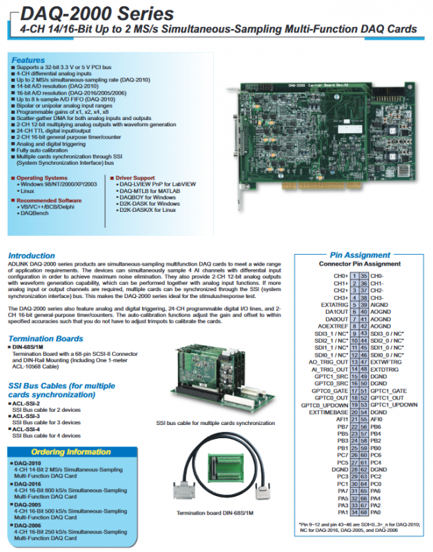
ADLINK DAQ-2000 series synchronous acquisition card
Core positioning and overall characteristics of the product
Bus specification: 32-bit universal 3.3V/5V PCI bus, compatible with old-fashioned industrial control hosts;
Core competency: 4-channel fully differential synchronous analog input, synchronous acquisition to eliminate channel phase difference, suitable for multi-channel synchronous testing;
Integrated functions: 2-channel 12 bit waveform generation analog output, 24 TTL digital IO, 2-channel 16 bit timing counter;
Synchronous Expansion: Built in SSI system synchronous bus, paired with dedicated synchronous cable for multi card cascading synchronization;
Transmission mechanism: Both AI and AO support high-speed DMA transmission through scattered aggregation;
Calibration: Onboard fully automatic self calibration, no need to manually adjust the potentiometer;
Trigger system: analog trigger, digital external trigger, SSI bus synchronous trigger, supporting multiple acquisition modes such as pre/post/intermediate/delay/repetition.
Comparison of Core Parameters of Four Models
Simulate input core differences
Model ADC Resolution Single Channel Maximum Sampling Rate AI FIFO Depth
DAQ-2010 14 bit (no loss code) 2 MS/s 8k sampling points
DAQ-2016 16 bit (no loss code) 800 kS/s 512 sampling points
DAQ-2005 16 bit (no loss code) 500 kS/s 512 sampling points
DAQ-2006 16 bit (no loss code) 250 kS/s 512 sampling points
Full range of universal AI configurations
Channel: 4-channel pure differential input, input impedance 1G Ω/100pF, CMRR gain level 1 up to 85dB;
Programmable gain: × 1/× 2/× 4/× 8;
Range options:
Bipolar: ± 10V, ± 5V, ± 2.5V, ± 1.25V
Monopolar: 0~10V, 0~5V, 0~2.5V, 0~1.25V
Coupling: DC coupling; -3dB bandwidth: DAQ2010 is 1MHz, 2016/05/06 is 600kHz;
Error metric: Gain error ± 0.01% FS (2010 is ± 0.03% FS).
Analog output (AO, all series unified specification)
Channel: 2-channel 12 bit multiplication DAC waveform output;
The maximum update rate is 1MS/s, the setup time is 3 μ s to 0.5LSB, and the slew rate is 20V/μ s;
Output range: 0~10V/± 10V/0~external reference/± external reference;
Driving capability: Each channel has a maximum of 5mA and can drive a capacitive load of 1500pF;
FIFO cache with 2k points, supporting both DMA and PIO transfers;
Trigger method: software, external digital/analog, SSI synchronous trigger.
Digital I/O and Timer Counter
24 way DIO
Based on the 8255 chip, 5V TTL level, only supports program polling PIO read and write, divided into three groups of 8-bit ports PA/PB/PC, all of which are led out to the 68 pin interface.
2-channel 16 bit universal timing counter
Built in 40MHz reference clock, supporting up to 10MHz external clock input;
Each independent clock source, gate control, output, and up/down counting pin is externally led out;
Can be used for frequency measurement, pulse generation, and external clock synchronization.
Self calibration hardware design
Onboard high-precision+5V reference voltage source, with a temperature drift of only ± 2ppm/℃;
Long term stability at 6ppm/1000 hours;
Fully automatic gain and offset calibration, no need for external standard sources, eliminating the need for hardware potentiometer debugging.
Trigger the complete system
trigger source
Software trigger, external simulation trigger, external digital trigger, SSI bus synchronization trigger.
Support collection mode
Pre trigger, post trigger, intermediate trigger, delayed trigger, repeated trigger, adapted for capturing shock, vibration, and transient signals.
Matching terminal board and synchronous accessories
DIN-68S/1M terminal board: 68 pin SCSI-II interface, supports DIN rail installation, comes standard with 1-meter ACL-10568 cable;
SSI synchronous cables: ACL-SSI-2 (dual card), ACL-SSI-3 (triple card), ACL-SSI-4 (quad card), multi card synchronous acquisition eliminates phase offset.
68 pin VHDCI connector pin definition
The interface is divided into four categories of signals:
AI differential: CHO~CH3 positive and negative inputs, analog ground AIGND;
AO dual output, external reference AOEXTREF, analog ground AOGND;
Digital trigger: EXTATRIG analog external trigger, EXTDTRIG digital external trigger, AO/AI trigger output;
Counter: GPTC0/1 clock, gate control, output, up and down counting pins;
DIO: PA/PB/PC three group 24 channel TTL, digital ground DGND;
SDI synchronous differential signal (only DAQ-2010 dedicated, other models are empty NC);
External reference clock EXTTIMEBASE.
Software Drivers and Development Environment
Operating system support
Windows 98/NT/2000/XP/2003, Linux system.
Development libraries and tools
D2K-DASK (Windows low-level C library), D2K-DASK/X (Linux driver);
DAQ-LabVIEW: LabVIEW specific VI driver;
DAQ-MTLB: MATLAB Acquisition Toolbox;
DAQBOY: Simple upper level testing software;
Programming language support: VB, VC++, BCB, Delphi.
Mechanical, environmental, and electrical power consumption
Size: 175mm × 107mm (excluding connector), 68 pin VHDCI female port;
Working temperature: 0~55 ℃; Storage -20~70 ℃; Humidity of 5-95% without condensation;
3 complete machines+5V power supply Typical current:
DAQ-2010:1.82A
DAQ-2016:2.26A
DAQ-2005:2.04A
DAQ-2006:1.82A